FUNCTIONAL DEVICE OPERATION
LOGIC COMMANDS AND REGISTERS
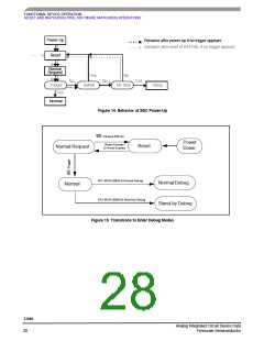
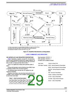
WD: Time-out 350 ms
Wake-up
Wake-up
Reset Counter
(3.4 ms) Expired
Reset
Sleep
Normal Request
Stop (1)
R
R
R
R
R
R
Normal
Stop Debug
Stand-by
E
E
SPI: Stand-by Debug
SPI: Normal Debug
Normal Debug
Stand-by Debug
R
R
(1) If Stop mode entered, it is entered without watchdog, no matter the WDSTOP bit.
(E) Debug mode entry point (Step 5 of the Debug mode entering sequence).
(R) Represents transitions to Reset mode due to V
low.
DD1
Figure 16. Simplified State Machine in Debug Modes
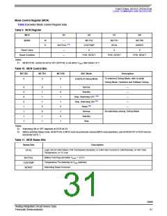
LOGIC COMMANDS AND REGISTERS
Read operation: R/W Bit = 0
Write operation: R/W Bit = 1
Possible reset conditions include:
SPI INTERFACE AND REGISTER DESCRIPTION
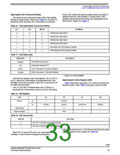
Table 7 illustrates a register, an 8-bit SPI. The first three
bits are used to identify the internal SBC register address. Bit
four is a read/write bit. The last four bits are Data Send from
MCU to SBC, or read back from SBC to MCU.
SBC Reset:
Power-On Reset POR
There is no significance during write operation state of
MISO.
SBC Mode Transition: NR2R - Normal Request to Reset Mode
NR2N - Normal Request to Normal Mode
During read operation only the final four bits of MISO have
a meaning (content of the accessed register).
NR2STB - Normal Request to Standby
Mode
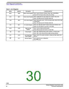
The following tables describe the SPI register list, and
register bit meaning.
N2R - Normal to Reset Mode
STB2R - Standby to Reset Mode
STO2R - Stop to Reset Mode
STO2NR - Stop to Normal Request
Registers reset value is also described along with the reset
condition. Reset condition is the condition causing the bit to
be set at the reset value.
Table 7. Data Format Description
Bit 7 Bit 6 Bit 5 Bit 4 Bit 3 Bit 2 Bit 1 Bit 0
SBC Mode:
RESET - SBC in Reset Mode
A2
A1
A0 R/W D3
D2
D1
D0
33989
Analog Integrated Circuit Device Data
Freescale Semiconductor
29

 FREESCALE [ Freescale ]