FUNCTIONAL DEVICE OPERATION
RESET AND WATCHDOG PINS, SOFTWARE WATCHDOG OPERATIONS
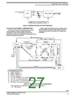
VDD1
RST
WD
VSUP (Open or > 5.0 V
Programming Bus
SBC
MCU = Flash
External supply and sources applied to VDD1, RST,
and WD test points on application circuit board.
Figure 12. Simplified Schematic for Flash Programming
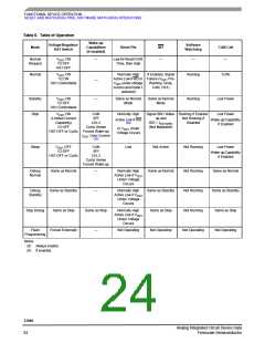
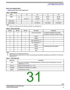
Table 6, page 24, describes the SBC operation modes.
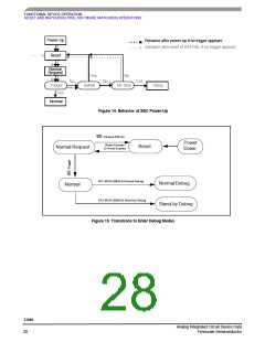
PACKAGE AND THERMAL CONSIDERATION
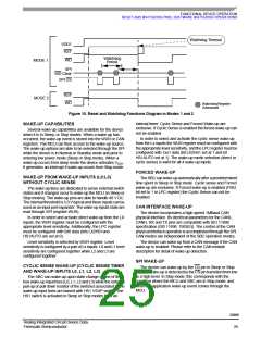
Normal, Stand-by, and Stop Debug modes are entered
through special sequence described in the Debug mode
paragraph.
The device is proposed in a standard surface mount
SOIC28 package. In order to improve the thermal
performances of the SOIC28 package, eight pins are
internally connected to the lead frame and are used for heat
transfer to the printed circuit board.
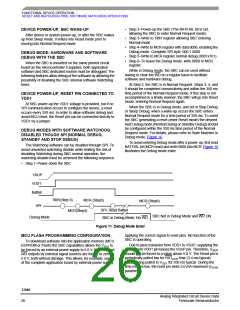
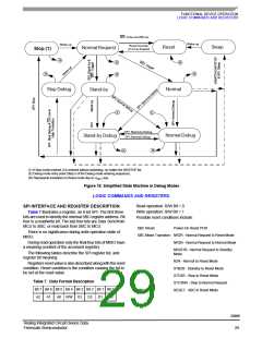
WD: Timeout OR V
Low
DD1
WD: Timeout
&
Nostop
2
SPI:Stand-by
& WD Trigger
Reset Counter (3.4
ms) Expired
1
3
Stand-by
Reset
Normal
1
V
Low OR WD:
DD1
4
Timeout 350 ms
&!Nostop
2
Power
Down
1
Normal
Stop
SPI: Stop & CS
Low to High
Transition
1
WD: Timeout OR V
Low
DD1
Wake-up
(V
DD1
High Temperature OR (V
1 Low > 100ms & V >BFew)) & Nostop &!BATFAIL
DD1 SUP
Sleep
denotes priority
1
2
3
4
STATE MACHINE DESCRIPTION:
28. Nostop = Nostop bit = 1
29. ! Nostop = Nostop bit = 0
30. BATFAIL = Batfail bit = 1
31. ! BATFAIL = Batfail bit = 0
32.
33.
34.
V
V
V
Over Temperature = V
thermal shutdown occurs
DD1
DD1
DD1
DD1
low = V
below reset threshold
DD1
low >100 ms = V
below reset threshold for more than 100 ms
DD1
35. WD: Trigger = TIM1 register write operation.
Figure 13. State Machine (Not Valid in Debug Modes)
Notes These two SPI commands must be sent consecutively in this sequence.
30. If WD activated.
33989
Analog Integrated Circuit Device Data
Freescale Semiconductor
27

 FREESCALE [ Freescale ]