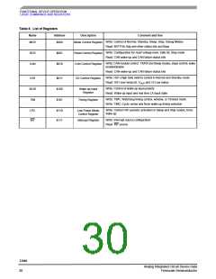
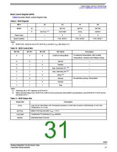
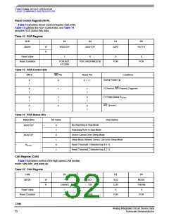
FUNCTIONAL DEVICE OPERATION
LOGIC COMMANDS AND REGISTERS
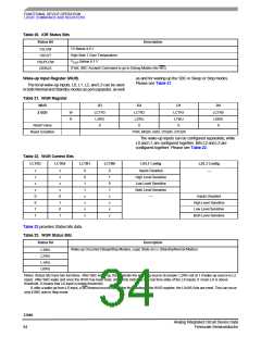
Table 20. IOR Status Bits
Status Bit
Description
V2 Below 4.0 V
High Side 1 Over Temperature
Below 6.1 V
V2LOW
HS1OT
V
VSUPLOW
DEBUG
SUP
If Set, SBC Accepts Command to go to Debug Modes (No WD)
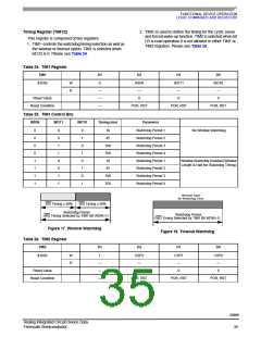
Wake-up Input Register (WUR)
as and for waking up the SBC in Sleep or Stop modes.
Please see Table 21.
The local wake-up inputs, L0, L1, L2, and L3 can be used
in both Normal and Standby modes as port expander, as well
Table 21. WUR Register
WUR
D3
D2
D1
D0
$100B
W
R
LCTR3
L3WU
0
LCTR2
L2WU
0
LCTR1
L1WU
0
LCTR0
L0WU
0
Reset Value
Reset Condition
POR, NR2R, N2R, STB2R, STO2R
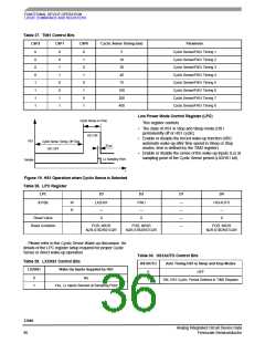
The wake-up inputs can be configured separately, while
L0 and L1 are configured together. Bits L2 and L3 are
configured together. Please see Table 22.
Table 22. WUR Control Bits
LCTR3
LCTR2
LCTR1
LCTR0
L0/L1 Config
L2/L3 Config
x
x
x
x
0
0
1
1
x
x
x
x
0
1
0
1
0
0
1
1
x
x
x
x
0
1
0
1
x
x
x
x
Inputs Disabled
High Level Sensitive
Low Level Sensitive
Both Level Sensitive
—
—
Inputs Disabled
High Level Sensitive
Low Level Sensitive
Both Level Sensitive
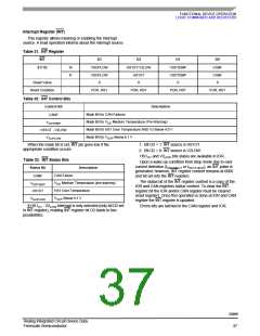
Table 23 provides Status bits data.
Table 23. WUR Status Bits
Status Bit
Description
Wake-up Occurred (Sleep/Stop Modes), Logic State on Lx (Standby/Normal Modes)
L3WU
L2WU
L1WU
L0WU
Notes: Status bits have two functions. After SBC wake-up, they indicate the wake-up source (Example: L2WU set at 1 if wake-up source is L2
input). After SBC wake and once the WUR has been read, status bits indicates the real time state of the LX inputs (1 mean LX is above
threshold, 0 means that LX input is below threshold).
If, after a wake-up from LX input, a WD timeout occurs before the first reading of the WUR register, the LXxWU bits are reset. This can occur
only if SBC was in Stop mode.
33989
Analog Integrated Circuit Device Data
34
Freescale Semiconductor

 FREESCALE [ Freescale ]