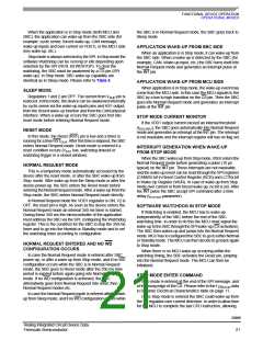
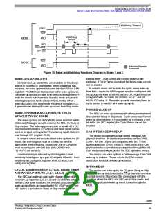
FUNCTIONAL DEVICE OPERATION
RESET AND WATCHDOG PINS, SOFTWARE WATCHDOG OPERATIONS
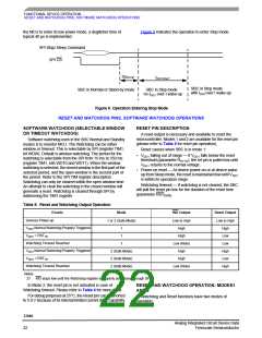
Watchdog Timeout
VDD1
RST
Watchdog
Period
WD
MODE 1
SPI
WD Clear
SPI CS
RST
WD
MODE 2
WatchdogRegister
Addressed
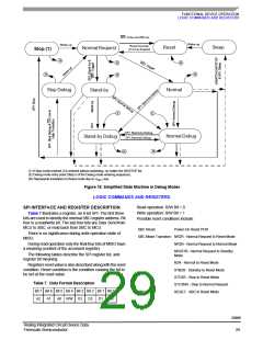
Figure 10. Reset and Watchdog Functions Diagram in Modes 1 and 2
internal timer. Cyclic Sense and Forced Wake-up are
exclusive. If Cyclic Sense is enabled the forced wake-up can
not be enabled.
WAKE-UP CAPABILITIES
Several wake-up capabilities are available for the device
when it is in Sleep, or Stop modes. When a wake-up has
occurred, the wake-up event is stored into the WUR or CAN
registers. The MCU can then access to the wake-up source.
The wake-up options are able to be selected through the SPI
while the device is in Normal or Standby mode and prior to
entering low power mode (Sleep or Stop mode). When a
In order to select and activate the cyclic sense wake-up
from the Lx inputs the WUR register must be configured with
the appropriate level sensitivity, and the LPC register must be
configured with 1xx1 data (bit LX2HS1 set at 1 and bit
HS1AUTO set at 1). The wake-up mode selection (direct or
cyclic sense) is valid for all 4 wake-up inputs.
wake-up occurs from sleep mode the device activates VDD1
.
It generates an interrupt if wake-up occurs from Stop mode.
FORCED WAKE-UP
WAKE-UP FROM WAKE-UP INPUTS (L0:L3)
WITHOUT CYCLIC SENSE
The SBC can wake-up automatically after a predetermined
time spent in Sleep or Stop mode. Cyclic sense and Forced
wake-up are exclusive. If Forced wake-up is enabled (FWU
bit set to 1 in LPC register) the Cyclic Sense can not be
enabled.
The wake-up lines are dedicated to sense external switch
states and if changes occur to wake-up the MCU (in Sleep or
Stop modes). The wake-up pins are able to handle 40 V DC.
The internal threshold is 3.0 V typical and these inputs can be
used as an input port expander. The wake-up inputs state are
read through SPI (register WUR).
CAN INTERFACE WAKE-UP
The device incorporates a high-speed 1MBaud CAN
physical interface. Its electrical parameters for the CANL,
CANH, RX and TX pins are compatible with ISO 11898
specification (IS0 11898: 1993(E)). The control of the CAN
physical interface operation is accomplished through the SPI.
CAN modes are independent of the SBC operation modes.
In order to select and activate direct wake-up from the LX
inputs, the WUR register must be configured with the
appropriate level sensitivity. Additionally, the LPC register
must be configured with 0x0 data (bits LX2HS1and
HS1AUTO are set at 0).
Level sensitivity is selected by WUR register. Level
sensitivity is configured by a pair of Lx inputs: L0 and L1 level
sensitivity are configured together while L2 and L3 are
configured together.
The device can wake-up from a CAN message if the CAN
wake-up is enabled. Please refer to the CAN module
description for detail of wake-up detection.
SPI WAKE-UP
CYCLIC SENSE WAKE-UP (CYCLIC SENSE TIMER
AND WAKE-UP INPUTS L0, L1, L2, L3)
The device can wake-up by the CS pin in Sleep or Stop
modes. Wake-up is detected by the CS pin transition from low
to a high level. In Stop mode, this corresponds with the
condition where the MCU and SBC are in Stop mode; and
when the application wake-up event comes through the
MCU.
The SBC can wake-up upon state change of one of the
four wake-up input lines (L0, L1, L2 and L3) while the external
pull-up or pull down resistor of the switches associated to the
wake-up input lines are biased with HS1 VSUP switch. The
HS1 switch is activated in Sleep or Stop modes from an
33989
Analog Integrated Circuit Device Data
Freescale Semiconductor
25

 FREESCALE [ Freescale ]