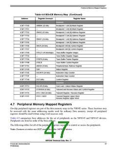
Peripheral Memory Mapped Registers
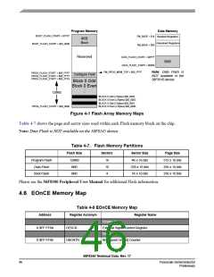
Table 4-8 EOnCE Memory Map (Continued)
Address
Register Acronym
Register Name
Reserved
X:$FF FF90
X:$FF FF91
X:$FF FF92
X:$FF FF93
X:$FF FF94
X:$FF FF95
X:$FF FF96
X:$FF FF97
X:$FF FF98
X:$FF FF99
X:$FF FF9A
X:$FF FF9B
X:$FF FF9C
X:$FF FF9D
X:$FF FF9E
X:$FF FF9F
X:$FF FFA0
OBMSK (32 bits)
Breakpoint 1 Unit [0] Mask Register
Breakpoint 1 Unit [0] Mask Register
Breakpoint 2 Unit [0] Address Register
Breakpoint 2 Unit [0] Address Register
Breakpoint 1 Unit [0] Address Register
Breakpoint 1 Unit [0] Address Register
Breakpoint Unit [0] Control Register
Breakpoint Unit [0] Control Register
Trace Buffer Register Stages
Trace Buffer Register Stages
Trace Buffer Pointer Register
Trace Buffer Control Register
Peripheral Base Address Register
Status Register
—
OBAR2 (32 bits)
—
OBAR1 (24 bits)
—
OBCR (24 bits)
—
OTB (21-24 bits/stage)
—
OTBPR (8 bits)
OTBCR
OBASE (8 bits)
OSR
OSCNTR (24 bits)
—
Instruction Step Counter
Instruction Step Counter
OCR (bits)
Control Register
Reserved
X:$FF FFFC
X:$FF FFFD
X:$FF FFFE
X:$FF FFFF
OCLSR (8 bits)
Core Lock / Unlock Status Register
Transmit and Receive Status and Control Register
Transmit Register / Receive Register
OTXRXSR (8 bits)
OTX / ORX (32 bits)
OTX1 / ORX1
Transmit Register Upper Word
Receive Register Upper Word
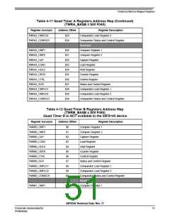
4.7 Peripheral Memory Mapped Registers
On-chip peripheral registers are part of the data memory map on the 56800E series. These locations may
be accessed with the same addressing modes used for ordinary Data memory, except all peripheral
registers should be read/written using word accesses only.
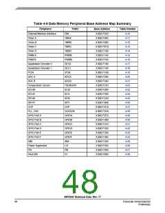
Table 4-9 summarizes base addresses for the set of peripherals on the 56F8345 and 56F8145 devices.
Peripherals are listed in order of the base address.
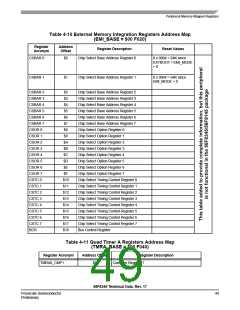
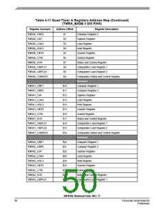
The following tables list all of the peripheral registers required to control or access the peripherals.
Note: Features in italics are NOT available in the 56F8145 device.
56F8345 Technical Data, Rev. 17
Freescale Semiconductor
Preliminary
47

 FREESCALE [ Freescale ]