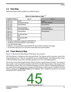
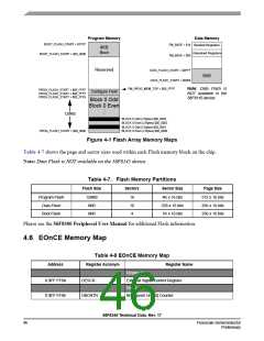
Data Memory
Program Memory
BOOT_FLASH_START + $1FFF
FM_BASE + $14
FM_BASE + $00
Banked Registers
8KB
Boot
Unbanked Registers
BOOT_FLASH_START = $02_0000
Reserved
DATA_FLASH_START + $0FFF
DATA_FLASH_START + $0000
8KB
Note: Data Flash is
NOT available in the
56F8145 device.
FM_PROG_MEM_TOP = $00_FFFF
PROG_FLASH_START + $00_FFFF
PROG_FLASH_START + $00_FFF7
PROG_FLASH_START + $00_FFF6
Configure Field
Block 0 Odd
Block 0 Even
128KB
BLOCK 0 Odd (2 Bytes) $00_0003
BLOCK 0 Even (2 Bytes) $00_0002
BLOCK 0 Odd (2 Bytes) $00_0001
BLOCK 0 Even (2 Bytes) $00_0000
PROG_FLASH_START = $00_0000
Figure 4-1 Flash Array Memory Maps
Table 4-7 shows the page and sector sizes used within each Flash memory block on the chip.
Note: Data Flash is NOT available on the 56F8145 device.
Table 4-7. Flash Memory Partitions
Flash Size
Sectors
Sector Size
Page Size
Program Flash
Data Flash
128KB
8KB
16
16
4
4K x 16 bits
256 x 16 bits
1K x 16 bits
512 x 16 bits
256 x 16 bits
256 x 16 bits
Boot Flash
8KB
Please see the 56F8300 Peripheral User Manual for additional Flash information.
4.6 EOnCE Memory Map
Table 4-8 EOnCE Memory Map
Address
Register Acronym
Register Name
Reserved
X:$FF FF8A
X:$FF FF8E
OESCR
External Signal Control Register
Reserved
OBCNTR
Breakpoint Unit [0] Counter
56F8345 Technical Data, Rev. 17
46
Freescale Semiconductor
Preliminary

 FREESCALE [ Freescale ]