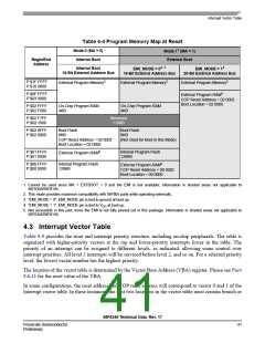
Data Map
4.4 Data Map
Note: Data Flash is NOT available on the 56F8145 device.
1, 2
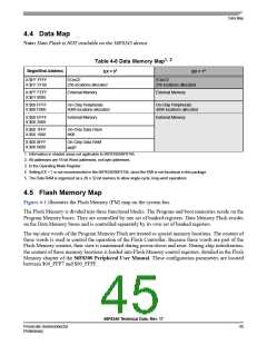
Table 4-6 Data Memory Map
EX = 03
EX = 14
Begin/End Address
X:$FF FFFF
X:$FF FF00
EOnCE
256 locations allocated
EOnCE
256 locations allocated
X:$FF FEFF
X:$01 0000
External Memory
External Memory
X:$00 FFFF
X:$00 F000
On-Chip Peripherals
4096 locations allocated
On-Chip Peripherals
4096 locations allocated
X:$00 EFFF
X:$00 2000
External Memory
External Memory
X:$00 1FFF
X:$00 1000
On-Chip Data Flash
8KB
X:$00 0FFF
X:$00 0000
On-Chip Data RAM
8KB5
1. Information in shaded areas not applicable to 56F8345/56F8145.
2. All addresses are 16-bit Word addresses, not byte addresses.
3. In the Operating Mode Register.
4. Setting EX = 1 is not recommended in the 56F8345/56F8145, since the EMI is not functional in this package.
5. The Data RAM is organized as a 2K x 32-bit memory to allow single-cycle, long-word operations.
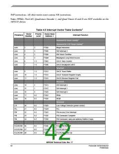
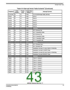
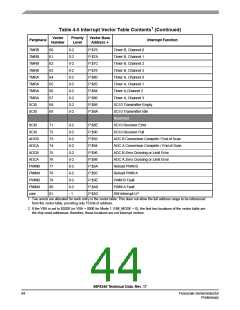
4.5 Flash Memory Map
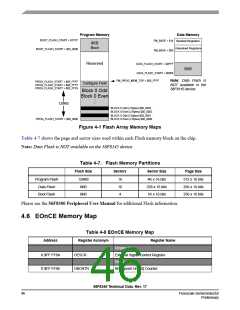
Figure 4-1 illustrates the Flash Memory (FM) map on the system bus.
The Flash Memory is divided into three functional blocks. The Program and boot memories reside on the
Program Memory buses. They are controlled by one set of banked registers. Data Memory Flash resides
on the Data Memory buses and is controlled separately by its own set of banked registers.
The top nine words of the Program Memory Flash are treated as special memory locations. The content of
these words is used to control the operation of the Flash Controller. Because these words are part of the
Flash Memory content, their state is maintained during power-down and reset. During chip initialization,
the content of these memory locations is loaded into Flash Memory control registers, detailed in the Flash
Memory chapter of the 56F8300 Peripheral User Manual. These configuration parameters are located
between $00_FFF7 and $00_FFFF.
56F8345 Technical Data, Rev. 17
Freescale Semiconductor
Preliminary
45

 FREESCALE [ Freescale ]