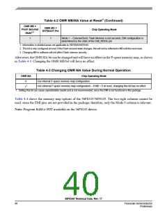
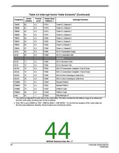
1
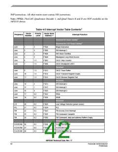
Table 4-5 Interrupt Vector Table Contents (Continued)
Vector
Number
Priority
Level
Vector Base
Address +
Peripheral
Interrupt Function
TMRB
TMRB
TMRB
TMRB
TMRA
TMRA
TMRA
TMRA
SCI0
60
0-2
P:$78
P:$7A
P:$7C
P:$7E
P:$80
P:$82
P:$84
P:$86
P:$88
P:$8A
Timer B, Channel 0
Timer B, Channel 1
Timer B, Channel 2
Timer B, Channel 3
Timer A, Channel 0
Timer A, Channel 1
Timer A,Channel 2
Timer A, Channel 3
61
62
63
64
65
66
67
68
69
0-2
0-2
0-2
0-2
0-2
0-2
0-2
0-2
0-2
SCI 0 Transmitter Empty
SCI 0 Transmitter Idle
Reserved
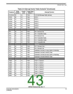
SCI0
SCI0
71
72
73
74
75
76
77
78
79
80
81
0-2
0-2
0-2
0-2
0-2
0-2
0-2
0-2
0-2
0-2
- 1
P:$8E
P:$90
P:$92
P:$94
P:$96
P:$98
P:$9A
P:$9C
P:$9E
P:$A0
P:$A2
SCI 0 Receiver Error
SCI0
SCI 0 Receiver Full
ADCB
ADCA
ADCB
ADCA
PWMB
PWMA
PWMB
PWMA
core
ADC B Conversion Compete / End of Scan
ADC A Conversion Complete / End of Scan
ADC B Zero Crossing or Limit Error
ADC A Zero Crossing or Limit Error
Reload PWM B
Reload PWM A
PWM B Fault
PWM A Fault
SW Interrupt LP
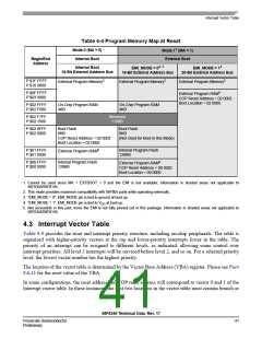
1. Two words are allocated for each entry in the vector table. This does not allow the full address range to be referenced
from the vector table, providing only 19 bits of address.
2. If the VBA is set to $0200 (or VBA = 0000 for Mode 1, EMI_MODE = 0), the first two locations of the vector table are
the chip reset addresses; therefore, these locations are not interrupt vectors.
56F8345 Technical Data, Rev. 17
44
Freescale Semiconductor
Preliminary

 FREESCALE [ Freescale ]