Interrupt Vector Table
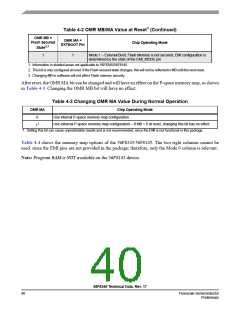
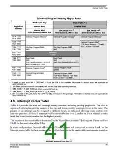
Table 4-4 Program Memory Map at Reset
Mode 11 (MA = 1)
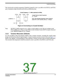
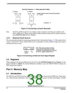
Mode 0 (MA = 0)
Internal Boot
Begin/End
Address
External Boot
EMI_MODE = 02, 3
EMI_MODE = 14
20-Bit External Address Bus
Internal Boot
16-Bit External Address Bus
16-Bit External Address Bus
External Program Memory5
External Program Memory5
External Program Memory5
P:$1F FFFF
P:$10 0000
External Program RAM5
COP Reset Address = 02 0002
Boot Location = 02 0000
P:$0F FFFF
P:$03 0000
P:$02 FFFF
P:$02 F800
On-Chip Program RAM
4KB
On-Chip Program RAM
4KB
P:$02 F7FF
P:$02 1000
Reserved
116KB
P:$02 0FFF
P:$02 0000
Boot Flash
8KB
Boot Flash
8KB
COP Reset Address = 02 0002
Boot Location = 02 0000
(Not Used for Boot in this Mode)
External Program RAM5
P:$01 FFFF
P:$01 0000
Internal Program Flash
128KB
External Program RAM5
COP Reset Address = 00 0002
Boot Location = 00 0000
P:$00 FFFF
P:$00 0000
Internal Program Flash
128KB
1. Cannot be used since MA = EXTBOOT = 0 and the EMI is not available; information in shaded areas not applicable to
56F8345/56F8145.
2. This mode provides maximum compatibility with 56F80x parts while operating externally.
3. “EMI_MODE = 0”, EMI_MODE pin is tied to ground at boot up.
4. “EMI_MODE = 1”, EMI_MODE pin is tied to V at boot up.
DD
5. Not accessible in this part, since the EMI is not fully pinned out in this package; information in shaded areas not applicable to
56F8345/56F8145.
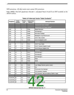
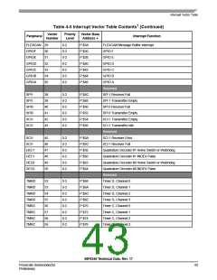
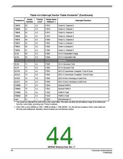
4.3 Interrupt Vector Table
Table 4-5 provides the reset and interrupt priority structure, including on-chip peripherals. The table is
organized with higher-priority vectors at the top and lower-priority interrupts lower in the table. The
priority of an interrupt can be assigned to different levels, as indicated, allowing some control over
interrupt priorities. All level 3 interrupts will be serviced before level 2, and so on. For a selected priority
level, the lowest vector number has the highest priority.
The location of the vector table is determined by the Vector Base Address (VBA) register. Please see Part
5.6.11 for the reset value of the VBA.
In some configurations, the reset address and COP reset address will correspond to vector 0 and 1 of the
interrupt vector table. In these instances, the first two locations in the vector table must contain branch or
56F8345 Technical Data, Rev. 17
Freescale Semiconductor
Preliminary
41

 FREESCALE [ Freescale ]