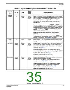
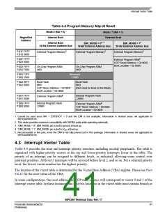
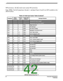
Program Map
RAM and Flash memories are used in both spaces.
This section provides memory maps for:
•
•
Program Address Space, including the Interrupt Vector Table
Data Address Space, including the EOnCE Memory and Peripheral Memory Maps
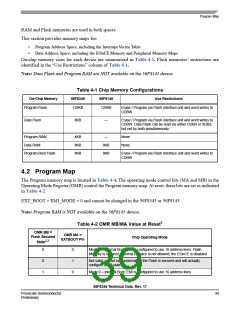
On-chip memory sizes for each device are summarized in Table 4-1. Flash memories’ restrictions are
identified in the “Use Restrictions” column of Table 4-1.
Note: Data Flash and Program RAM are NOT available on the 56F8145 device.
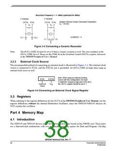
Table 4-1 Chip Memory Configurations
On-Chip Memory
56F8345
56F8145
Use Restrictions
Program Flash
128KB
128KB
Erase / Program via Flash interface unit and word writes to
CDBW
Data Flash
8KB
—
Erase / Program via Flash interface unit and word writes to
CDBW. Data Flash can be read via either CDBR or XDB2,
but not by both simultaneously
Program RAM
Data RAM
4KB
8KB
8KB
—
None
None
8KB
8KB
Program Boot Flash
Erase / Program via Flash Interface unit and word writes to
CDBW
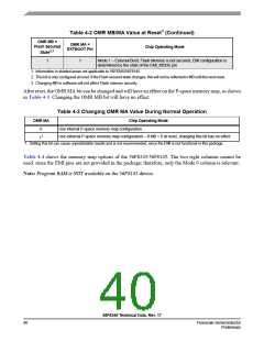
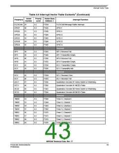
4.2 Program Map
The Program memory map is located in Table 4-4. The operating mode control bits (MA and MB) in the
Operating Mode Register (OMR) control the Program memory map. At reset, these bits are set as indicated
in Table 4-2.
EXT_BOOT = EMI_MODE = 0 and cannot be changed in the 56F8345 or 56F8145.
Note: Program RAM is NOT available on the 56F8145 device.
1
Table 4-2 OMR MB/MA Value at Reset
OMR MB =
OMR MA =
Flash Secured
State2,3
Chip Operating Mode
EXTBOOT Pin
0
0
1
0
Mode 0 – Internal Boot; EMI is configured to use 16 address lines; Flash
Memory is secured; external P-space is not allowed; the EOnCE is disabled
1
0
Not valid; cannot boot externally if the Flash is secured and will actually
configure to 00 state
Mode 0 – Internal Boot; EMI is configured to use 16 address lines
56F8345 Technical Data, Rev. 17
Freescale Semiconductor
Preliminary
39

 FREESCALE [ Freescale ]