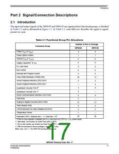
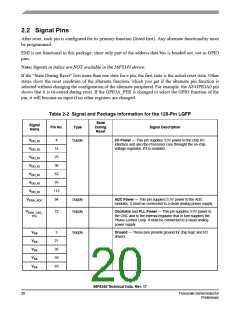
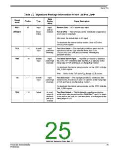
Signal Pins
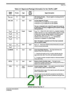
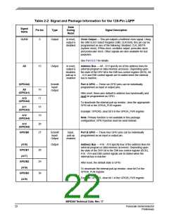
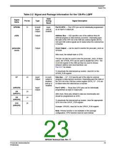
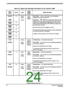
Table 2-2 Signal and Package Information for the 128-Pin LQFP
State
During
Reset
Signal
Name
Pin No.
Type
Signal Description
VSSA_ADC
OCR_DIS
95
71
Supply
Input
ADC Analog Ground — This pin supplies an analog ground to
the ADC modules.
Input
On-Chip Regulator Disable —
Tie this pin to VSS to enable the on-chip regulator
Tie this pin to VDD to disable the on-chip regulator
This pin is intended to be a static DC signal from power-up
to shut down. Do not try to toggle this pin for power savings
during operation.
VCAP
VCAP
VCAP
VCAP
1
2
3
4
49
122
75
Supply
Supply
VCAP1 - 4 — When OCR_DIS is tied to VSS (regulator enabled),
connect each pin to a 2.2μF or greater bypass capacitor in order
to bypass the core logic voltage regulator, required for proper
chip operation. When OCR_DIS is tied to VDD (regulator
disabled), these pins become VDD_CORE and should be
connected to a regulated 2.5V power supply.
13
Note: This bypass is required even if the chip is powered
with an external supply.
V
PP1
119
5
Input
Input
Input
Input
VPP1 - 2 — These pins should be left unconnected as an open
circuit for normal functionality.
VPP
2
CLKMODE
79
Clock Input Mode Selection — This input determines the
function of the XTAL and EXTAL pins.
1 = External clock input on XTAL is used to directly drive the
input clock of the chip. The EXTAL pin should be grounded.
0 = A crystal or ceramic resonator should be connected between
XTAL and EXTAL.
EXTAL
XTAL
74
73
Input
Input
External Crystal Oscillator Input — This input can be
connected to an 8MHz external crystal. Tie this pin low if XTAL is
driven by an external clock source.
Input/
Chip-driven Crystal Oscillator Output — This output connects the internal
Output
crystal oscillator output to an external crystal.
If an external clock is used, XTAL must be used as the input and
EXTAL connected to GND.
The input clock can be selected to provide the clock directly to
the core. This input clock can also be selected as the input clock
for the on-chip PLL.
56F8345 Technical Data, Rev. 17
Freescale Semiconductor
Preliminary
21

 FREESCALE [ Freescale ]