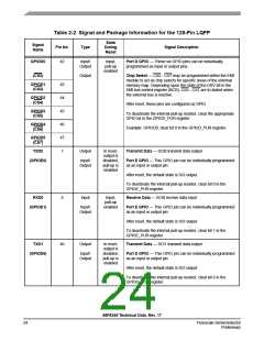
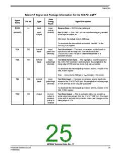
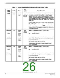
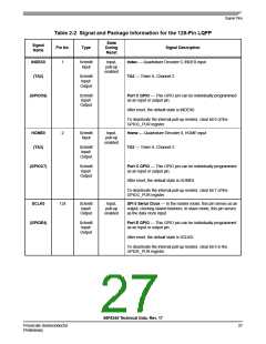
Table 2-2 Signal and Package Information for the 128-Pin LQFP
State
During
Reset
Signal
Name
Pin No.
Type
Signal Description
GPIOD0
42
Input/
Output
Input,
pull-up
enabled
Port D GPIO — These six GPIO pins can be individually
programmed as input or output pins.
(CS2)
Output
Chip Select — CS2 - CS7 may be programmed within the EMI
module to act as chip selects for specific areas of the external
memory map. Depending upon the state of the DRV bit in the
EMI bus control register (BCR), CS2 - CS7 are tri-stated when
the external bus is inactive.
GPIOD1
(CS3)
43
44
45
46
47
7
GPIOD2
(CS4)
After reset, these pins are configured as GPIO.
GPIOD3
(CS5)
To deactivate the internal pull-up resistor, clear the appropriate
GPIO bit in the GPIOD_PUR register.
GPIOD4
(CS6)
Example: GPIOD0, clear bit 0 in the GPIOD_PUR register.
GPIOD5
(CS7)
TXD0
Output
In reset,
output is
disabled,
pull-up is
enabled
Transmit Data — SCI0 transmit data output
(GPIOE0)
Input/
Output
Port E GPIO — This GPIO pin can be individually programmed
as an input or output pin.
After reset, the default state is SCI output.
To deactivate the internal pull-up resistor, clear bit 0 in the
GPIOE_PUR register.
RXD0
8
Input
Input,
pull-up
enabled
Receive Data — SCI0 receive data input
(GPIOE1)
Input/
Port E GPIO — This GPIO pin can be individually programmed
Output
as an input or output pin.
After reset, the default state is SCI output.
To deactivate the internal pull-up resistor, clear bit 1 in the
GPIOE_PUR register.
TXD1
40
Output
In reset,
output is
disabled,
pull-up is
enabled
Transmit Data — SCI1 transmit data output
(GPIOD6)
Input/
Output
Port D GPIO — This GPIO pin can be individually programmed
as an input or output pin.
After reset, the default state is SCI output.
To deactivate the internal pull-up resistor, clear bit 6 in the
GPIOD_PUR register.
56F8345 Technical Data, Rev. 17
24
Freescale Semiconductor
Preliminary

 FREESCALE [ Freescale ]