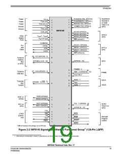
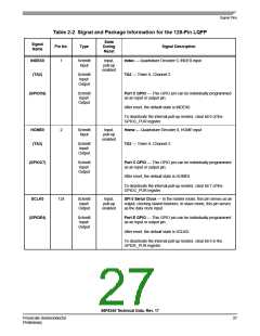
Signal Pins
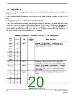
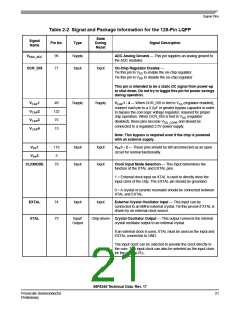
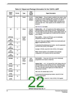
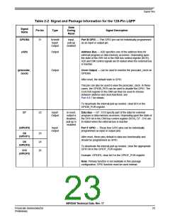
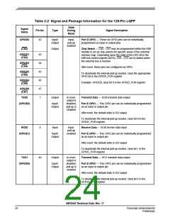
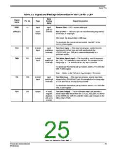
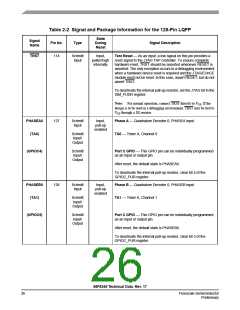
Table 2-2 Signal and Package Information for the 128-Pin LQFP
State
During
Reset
Signal
Name
Pin No.
Type
Signal Description
GPIOB4
(A20)
31
Schmitt
Input/
Output
Input,
pull-up
enabled
Port B GPIO — This GPIO pin can be individually programmed
as an input or output pin.
Output
Address Bus — A20 specifies one of the address lines for
external program or data memory accesses. Depending upon
the state of the DRV bit in the EMI bus control register (BCR),
A20 and EMI control signals are tri-stated when the external bus
is inactive.
(prescaler_
clock)
Output
Clock Output — can be used to monitor the prescaler_clock on
GPIOB4.
After reset, the default state is GPIO.
This pin can also be used to view the prescaler_clock. In these
cases, the GPIOB_PER can be used to disable the GPIO. The
CLKOSR register in the SIM can then be used to choose
between address and clock functions; see
Part 6.5.7 for details.
To deactivate the internal pull-up resistor, clear bit 4 in the
GPIOB_PUR register.
D7
22
Input/
Output
In reset,
output is
disabled,
pull-up is
enabled
Data Bus — D7 - D10 specify part of the data for external
program or data memory accesses. Depending upon the state of
the DRV bit in the EMI bus control register (BCR), D7 - D10 are
tri-stated when the external bus is inactive
(GPIOF0)
Input/
Port F GPIO — These four GPIO pins can be individually
Output
programmed as input or output pins.
D8
(GPIOF1)
23
24
26
After reset, these pins default to data bus functionality and
should be programmed as GPIO.
D9
(GPIOF2)
To deactivate the internal pull-up resistor, clear the appropriate
GPIO bit in the GPIOF_PUR register.
D10
(GPIOF3)
Example: GPIOF0, clear bit 0 in the GPIOF_PUR register.
Note: Primary function is not available in this package
configuration; GPIO function must be used instead.
56F8345 Technical Data, Rev. 17
Freescale Semiconductor
Preliminary
23

 FREESCALE [ Freescale ]