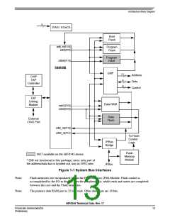
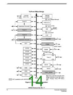
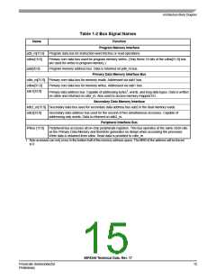
Introduction
Part 2 Signal/Connection Descriptions
2.1 Introduction
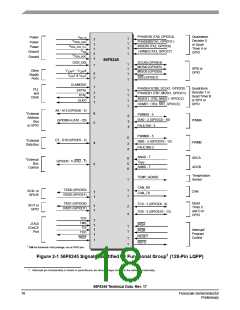
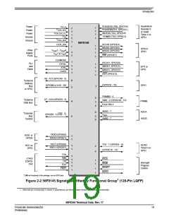
The input and output signals of the 56F8345 and 56F8145 are organized into functional groups, as detailed
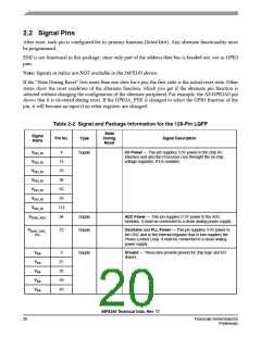
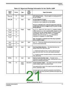
in Table 2-1 and as illustrated in Figure 2-1. In Table 2-2, each table row describes the signal or signals
present on a pin.
Table 2-1 Functional Group Pin Allocations
Number of Pins in Package
Functional Group
56F8345
56F8145
Power (VDD or VDDA
)
9
1
6
6
9
1
6
6
Power Option Control
Ground (VSS or VSSA
)
Supply Capacitors1 & VPP
PLL and Clock
4
6
4
6
Bus Control
Interrupt and Program Control
Pulse Width Modulator (PWM) Ports
Serial Peripheral Interface (SPI) Port 0
Serial Peripheral Interface (SPI) Port 1
4
4
26
4
13
4
—
4
4
Quadrature Decoder Port 02
4
Quadrature Decoder Port 13
Serial Communications Interface (SCI) Ports
CAN Ports
4
—
4
2
4
—
21
4
Analog-to-Digital Converter (ADC) Ports
Timer Module Ports
21
6
JTAG/Enhanced On-Chip Emulation (EOnCE)
Temperature Sense
5
5
1
—
28
Dedicated GPIO ( Address Bus = 11; Data Bus = 44)
28
1. If the on-chip regulator is disabled, the V
pins serve as 2.5V V
power inputs
DD_CORE
CAP
2. Alternately, can function as Quad Timer pins or GPIO
3. Pins in this section can function as Quad Timer, SPI 1, orGPIO
4. EMI not functional in these packages; use as GPIO pins.
Note: See Table 1-1 for 56F8145 functional differences.
56F8345 Technical Data, Rev. 17
Freescale Semiconductor
Preliminary
17

 FREESCALE [ Freescale ]