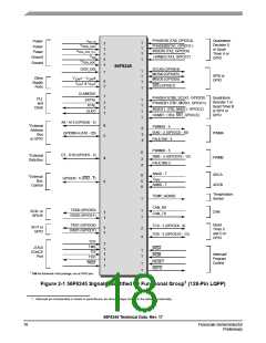
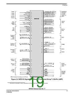
2.2 Signal Pins
After reset, each pin is configured for its primary function (listed first). Any alternate functionality must
be programmed.
EMI is not functional in this package; since only part of the address/data bus is bonded out, use as GPIO
pins.
Note: Signals in italics are NOT available in the 56F8145 device.
If the “State During Reset” lists more than one state for a pin, the first state is the actual reset state. Other
states show the reset condition of the alternate function, which you get if the alternate pin function is
selected without changing the configuration of the alternate peripheral. For example, the A8/GPIOA0 pin
shows that it is tri-stated during reset. If the GPIOA_PER is changed to select the GPIO function of the
pin, it will become an input if no other registers are changed.
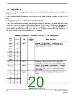
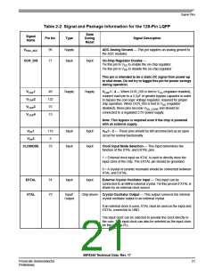
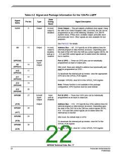
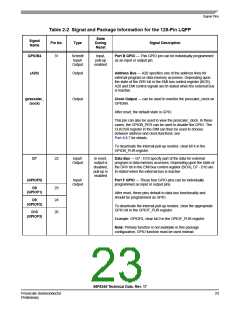
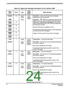
Table 2-2 Signal and Package Information for the 128-Pin LQFP
State
During
Reset
Signal
Name
Pin No.
Type
Signal Description
VDD_IO
VDD_IO
VDD_IO
VDD_IO
VDD_IO
VDD_IO
VDD_IO
VDDA_ADC
4
14
25
36
62
76
112
94
Supply
I/O Power — This pin supplies 3.3V power to the chip I/O
interface and also the Processor core throught the on-chip
voltage regulator, if it is enabled.
Supply
Supply
ADC Power — This pin supplies 3.3V power to the ADC
modules. It must be connected to a clean analog power supply.
VDDA_OSC_
72
Oscillator and PLL Power — This pin supplies 3.3V power to
the OSC and to the internal regulator that in turn supplies the
Phase Locked Loop. It must be connected to a clean analog
power supply.
PLL
VSS
VSS
VSS
VSS
VSS
3
Supply
Ground — These pins provide ground for chip logic and I/O
drivers.
21
35
59
65
56F8345 Technical Data, Rev. 17
20
Freescale Semiconductor
Preliminary

 FREESCALE [ Freescale ]