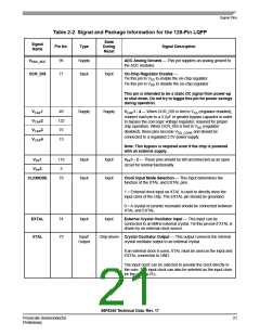
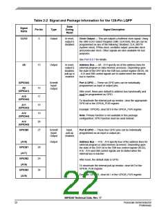
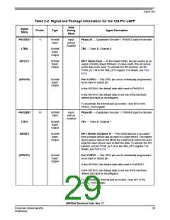
Signal Pins
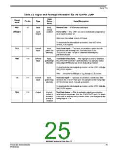
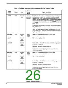
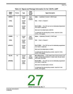
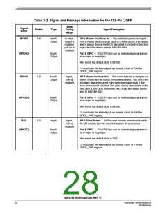
Table 2-2 Signal and Package Information for the 128-Pin LQFP
State
During
Reset
Signal
Name
Pin No.
Type
Signal Description
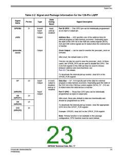
RXD1
41
Input
Input,
pull-up
enabled
Receive Data — SCI1 receive data input
(GPIOD7)
Input/
Port D GPIO — This GPIO pin can be individually programmed
Output
as an input or output pin.
After reset, the default state is SCI input.
To deactivate the internal pull-up resistor, clear bit 7 in the
GPIOD_PUR register.
TCK
TMS
115
116
Schmitt
Input
Input,
pulled low
internally
Test Clock Input — This input pin provides a gated clock to
synchronize the test logic and shift serial data to the
JTAG/EOnCE port. The pin is connected internally to a
pull-down resistor.
Schmitt
Input
Input,
pulled high
internally
Test Mode Select Input — This input pin is used to sequence
the JTAG TAP controller’s state machine. It is sampled on the
rising edge of TCK and has an on-chip pull-up resistor.
To deactivate the internal pull-up resistor, set the JTAG bit in the
SIM_PUDR register.
Note: Always tie the TMS pin to VDD through a 2.2K resistor.
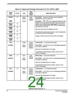
TDI
117
118
Schmitt
Input
Input,
pulled high
internally
Test Data Input — This input pin provides a serial input data
stream to the JTAG/EOnCE port. It is sampled on the rising edge
of TCK and has an on-chip pull-up resistor.
To deactivate the internal pull-up resistor, set the JTAG bit in the
SIM_PUDR register.
TDO
Output
In reset,
output is
disabled,
pull-up is
enabled
Test Data Output — This tri-stateable output pin provides a
serial output data stream from the JTAG/EOnCE port. It is driven
in the shift-IR and shift-DR controller states, and changes on the
falling edge of TCK.
56F8345 Technical Data, Rev. 17
Freescale Semiconductor
Preliminary
25

 FREESCALE [ Freescale ]