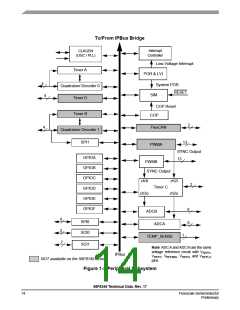
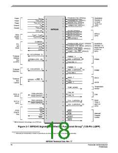
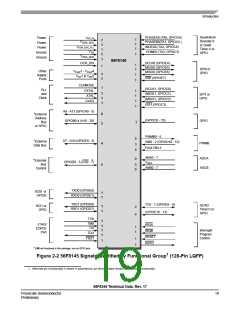
Quadrature
Decoder 0
or Quad
Timer A or
GPIO
V
PHASEA0 (TA0, GPIOC4)
PHASEB0(TA1, GPIOC5 )
INDEX0 (TA2, GPIOC6)
Power
Power
DD_IO
1
1
1
7
1
1
5
1
VDDA_ADC
V
DDA_OSC_PLL
VSS
Power
Ground
Ground
HOME0 (TA3, GPIOC7)
1
VSSA_ADC
56F8345
OCR_DIS
SCLK0 (GPIOE4)
MOSI0 (GPIOE5)
MISO0 (GPIOE6)
1
1
1
SPI0 or
GPIO
Other
Supply
Ports
V
CAP1 - VCAP
VPP1 & VPP
4
2
4
2
1
1
SS0 (GPIOE7)
CLKMODE
1
PHASEA1(TB0, SCLK1, GPIOC0)
PHASEB1 (TB1, MOSI1, GPIOC1)
Quadrature
Decoder 1 or
Quad Timer B
or SPI1 or
GPIO
PLL
and
Clock
EXTAL
XTAL
1
1
1
1
1
INDEX1 (TB2, MISO1, GPIOC2)
HOME1 (TB3, SS1, GPIOC3)
CLKO
1
1
A8 - A13 (GPIOA0 - 5)
GPIOB0-4 (A16 - 20)
6
5
*External
Address
Bus
PWMA0 - 5
6
3
4
ISA0 - 2 (GPIOC8 - 10)
PWMA
PWMB
or GPIO
FAULTA0 - 3
PWMB0 - 5
6
D7 - D10 (GPIOF0 - 3)
GPIOD0 - 5 (CS2 - 7)
*External
Data Bus
ISB0 - 2 (GPIOD10 - 12)
4
6
3
4
FAULTB0-3
ANA0 - 7
VREF
ADCA
ADCB
8
*External
Bus
Control
5
8
ANB0 - 7
Temperature
Sensor
TEMP_SENSE
1
CAN_RX
CAN_TX
TXD0 (GPIOE0)
RXD0 (GPIOE1)
1
1
SCI0 or
GPIOE
CAN
1
1
Quad
TXD1 (GPIOD6)
RXD1 (GPIOD7)
TC0 - 1 (GPIOE8 - 9)
SCI1 or
GPIO
1
1
2
4
Timer C
and D or
GPIO
TD0 - 3 (GPIOE10 - 13)
TCK
TMS
TDI
1
JTAG/
EOnCE
Port
IRQA
1
1
1
1
Interrupt/
Program
Control
IRQB
TDO
1
1
RESET
RSTO
TRST
1
1
* EMI not functional in this package; use as GPIO pins
1
Figure 2-1 56F8345 Signals Identified by Functional Group (128-Pin LQFP)
1. Alternate pin functionality is shown in parenthesis; pin direction/type shown is the default functionality.
56F8345 Technical Data, Rev. 17
18
Freescale Semiconductor
Preliminary

 FREESCALE [ Freescale ]