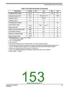
Analog-to-Digital Converter (ADC) Parameters
Table 10-23 ADC Parameters (Continued)
Characteristic
Symbol
VOFFSET
AECAL
CF1
Min
—
Typ
+/- 18
Max
+/- 46
—
Unit
mV
LSBs
—
Uncalibrated Offset Voltage
Calibrated Absolute Error6
Calibration Factor 17
—
See Figure 10-21
-0.003141
-17.6
—
—
Calibration Factor 27
CF2
—
—
—
Crosstalk between channels
Common Mode Voltage
—
—
—
-60
—
—
dB
V
Vcommon
(VREFH - VREFLO) / 2
Signal-to-noise ratio
SNR
SINAD
THD
—
—
—
—
—
64.6
59.1
60.6
61.1
9.6
—
—
—
—
—
db
db
Signal-to-noise plus distortion ratio
Total Harmonic Distortion
Spurious Free Dynamic Range
db
SFDR
ENOB
db
Effective Number Of Bits8
Bits
1. INL measured from V = .1V
to V = .9V
in REFH
in
REFH
10% to 90% Input Signal Range
2. LSB = Least Significant Bit
3. ADC clock cycles
4. Assumes each voltage reference pin is bypassed with 0.1μF ceramic capacitors to ground
5. The current that can be injected or sourced from an unselected ADC signal input without impacting the performance of
the ADC. This allows the ADC to operate in noisy industrial environments where inductive flyback is possible.
6. Absolute error includes the effects of both gain error and offset error.
7. Please see the 56F8300 Peripheral User’s Manual for additional information on ADC calibration.
8. ENOB = (SINAD - 1.76)/6.02
56F8345 Technical Data, Rev. 17
Freescale Semiconductor
Preliminary
153

 FREESCALE [ Freescale ]