Serial Communication Interface (SCI) Timing
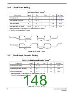
PPH PPH PPH PPH
Phase A
(Input)
PHL
PIN
PHL
Phase B
(Input)
PHL
PIN
PHL
Figure 10-14 Quadrature Decoder Timing
10.12 Serial Communication Interface (SCI) Timing
1
Table 10-20 SCI Timing
Characteristic
Baud Rate2
Symbol
BR
Min
—
Max
Unit
See Figure
—
(fMAX/16)
Mbps
RXD3 Pulse Width
TXD4 Pulse Width
RXDPW
TXDPW
0.965/BR
0.965/BR
1.04/BR
1.04/BR
ns
ns
10-15
10-16
1. Parameters listed are guaranteed by design.
2. f is the frequency of operation of the system clock, ZCLK, in MHz, which is 60MHz for the 56F8345 device and
MAX
40MHz for the 56F8145 device.
3. The RXD pin in SCI0 is named RXD0 and the RXD pin in SCI1 is named RXD1.
4. The TXD pin in SCI0 is named TXD0 and the TXD pin in SCI1 is named TXD1.
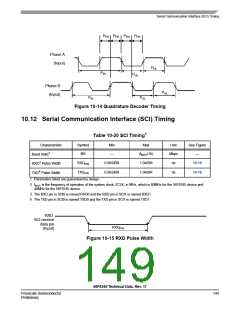
RXD
SCI receive
data pin
RXDPW
(Input)
Figure 10-15 RXD Pulse Width
56F8345 Technical Data, Rev. 17
Freescale Semiconductor
Preliminary
149

 FREESCALE [ Freescale ]