Equivalent Circuit for ADC Inputs
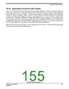
10.16 Equivalent Circuit for ADC Inputs
Figure 10-22 illustrates the ADC input circuit during sample and hold. S1 and S2 are always open/closed
at the same time that S3 is closed/open. When S1/S2 are closed & S3 is open, one input of the sample and
hold circuit moves to V
- V
/ 2, while the other charges to the analog input voltage. When the
REFH
REFH
switches are flipped, the charge on C1 and C2 are averaged via S3, with the result that a single-ended
analog input is switched to a differential voltage centered about V - V / 2. The switches switch
REFH
REFH
on every cycle of the ADC clock (open one-half ADC clock, closed one-half ADC clock). Note that there
are additional capacitances associated with the analog input pad, routing, etc., but these do not filter into
the S/H output voltage, as S1 provides isolation during the charge-sharing phase.
One aspect of this circuit is that there is an on-going input current, which is a function of the analog input
voltage, V
and the ADC clock frequency.
REF
56F8345 Technical Data, Rev. 17
Freescale Semiconductor
Preliminary
155

 FREESCALE [ Freescale ]