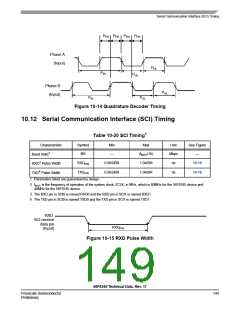
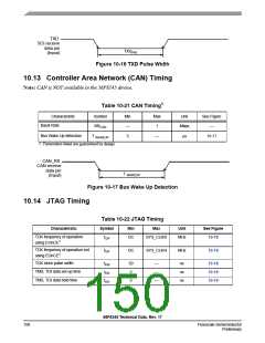
TXD
SCI receive
data pin
TXDPW
(Input)
Figure 10-16 TXD Pulse Width
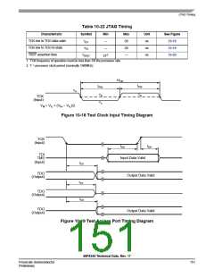
10.13 Controller Area Network (CAN) Timing
Note: CAN is NOT available in the 56F8145 device.
1
Table 10-21 CAN Timing
Characteristic
Baud Rate
Bus Wake Up detection
Symbol
BRCAN
Min
—
5
Max
1
Unit
See Figure
—
Mbps
T WAKEUP
μs
10-17
—
1. Parameters listed are guaranteed by design
CAN_RX
CAN receive
data pin
T WAKEUP
(Input)
Figure 10-17 Bus Wake Up Detection
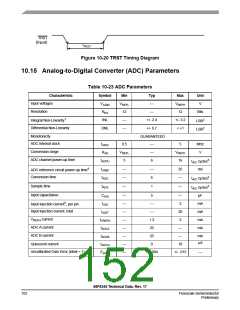
10.14 JTAG Timing
Table 10-22 JTAG Timing
Characteristic
Symbol
Min
Max
Unit
See Figure
10-18
TCK frequency of operation
using EOnCE1
fOP
DC
SYS_CLK/8
MHz
TCK frequency of operation not
using EOnCE1
fOP
DC
SYS_CLK/4
MHz
10-18
TCK clock pulse width
TMS, TDI data set-up time
TMS, TDI data hold time
tPW
tDS
tDH
50
5
—
—
—
ns
ns
ns
10-18
10-19
10-19
5
56F8345 Technical Data, Rev. 17
150
Freescale Semiconductor
Preliminary

 FREESCALE [ Freescale ]