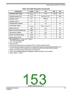
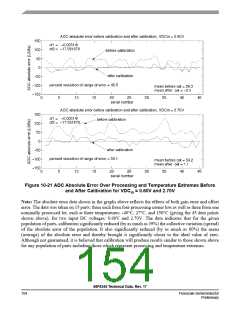
Figure 10-21 ADC Absolute Error Over Processing and Temperature Extremes Before
and After Calibration for VDC = 0.60V and 2.70V
in
Note: The absolute error data shown in the graphs above reflects the effects of both gain error and offset
error. The data was taken on 15 parts: three each from four processing corner lots as well as three from one
nominally processed lot, each at three temperatures: -40°C, 27°C, and 150°C (giving the 45 data points
shown above), for two input DC voltages: 0.60V and 2.70V. The data indicates that for the given
population of parts, calibration significantly reduced (by as much as 39%) the collective variation (spread)
of the absolute error of the population. It also significantly reduced (by as much as 80%) the mean
(average) of the absolute error and thereby brought it significantly closer to the ideal value of zero.
Although not guaranteed, it is believed that calibration will produce results similar to those shown above
for any population of parts including those which represent processing and temperature extremes.
56F8345 Technical Data, Rev. 17
154
Freescale Semiconductor
Preliminary

 FREESCALE [ Freescale ]