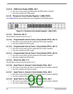
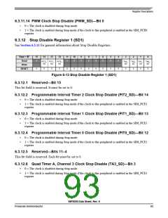
6.3.12.7 Quad Timer A, Channel 2 Clock Stop Disable (TA2_SD)—Bit 2
•
•
0 = The clock is disabled during Stop mode
1 = The clock is enabled during Stop mode if the clock to this peripheral is enabled in the SIM_PCE1
register
6.3.12.8 Quad Timer A, Channel 1 Clock Stop Disable (TA1_SD)—Bit 1
•
•
0 = The clock is disabled during Stop mode
1 = The clock is enabled during Stop mode if the clock to this peripheral is enabled in the SIM_PCE1
register
6.3.12.9 Quad Timer A, Channel 0 Clock Stop Disable (TA0_SD)—Bit 0
•
•
0 = The clock is disabled during Stop mode
1 = The clock is enabled during Stop mode if the clock to this peripheral is enabled in the SIM_PCE1
register
6.3.13 I/O Short Address Location Register High (SIM_IOSAHI)
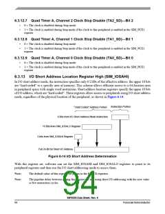
In I/O short address mode, the instruction specifies only 6 LSBs of the effective address; the upper 18 bits
are “hard coded” to a specific area of memory. This scheme allows efficient access to a 64-location area
in peripheral space with single word instruction. Short address location registers specify the upper 18 bits
of I/O address, which are “hard coded”. These registers allow access to peripherals using I/O short address
mode, regardless of the physical location of the peripheral, as shown in Figure 6-14.
Instruction Portion
“Hard Coded” Address Portion
6 Bits from I/O Short Address Mode Instruction
16 Bits from SIM_IOSALO Register
2 bits from SIM_IOSAHI Register
Full 24-Bit for Short I/O Address
Figure 6-14 I/O Short Address Determination
With this register set, software can set the SIM_IOSAHI and SIM_IOSALO registers to point to its
peripheral registers and then use the I/O short addressing mode to access them.
Note:
Note:
The default value of this register set points to the EOnCE registers.
The pipeline delay between setting this register set and using short I/O addressing with the new value
is five instruction cycles.
56F8036 Data Sheet, Rev. 6
94
FreescaleSemiconductor

 FREESCALE [ Freescale ]