Register Descriptions
GPIOA6_PEREN
Register
SIM_GPSA0
Register
GPIOA6
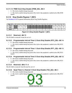
0
GPIOA6 pin
PWM
FAULT0
0
1
1
Timer A0
Figure 6-18 Overall Control of Signal Source Using SIM_GPSnn Control
In some cases, the user can choose peripheral function between several I/O, each of which have the option
to be programmed to control a specific peripheral function. If the user wishes to use that function, only one
of these I/O must be configured to control that peripheral function. If more than one I/O is configured to
control the peripheral function, the peripheral output signal will fan out to each I/O, but the peripheral input
signal will be the logical OR and AND of all the I/O signals.
Complete lists of I/O muxings are provided in Table 2-3.
The GPSn setting can be altered during normal operation, but a delay must be inserted between the time
when one function is disabled and another function is enabled.
Note:
After reset, all I/O pins are GPIO, except the JTAG pins and the RESET pin.
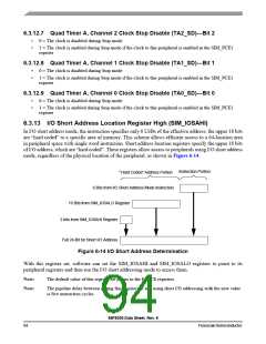
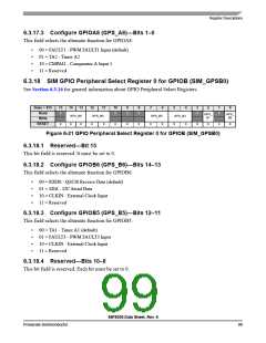
Base + $13
15
14
13
12
GPS_A6
0
11
10
9
8
7
6
5
4
3
2
1
0
0
0
0
0
0
0
0
0
0
0
0
Read
Write
GPS_A5
GPS_A4
RESET
0
0
0
0
0
0
0
0
0
0
0
0
0
0
0
Figure 6-19 GPIO Peripheral Select Register 0 for GPIOA (SIM_GPSA0)
6.3.16.1 Reserved—Bits 15–13
This bit field is reserved. Each bit must be set to 0.
6.3.16.2 Configure GPIOA6 (GPS_A6)—Bit 12
This field selects the alternate function for GPIOA6.
•
•
0 = FAULT0 - PWM FAULT0 Input (default)
1 = TA0 - Timer A0
56F8036 Data Sheet, Rev. 6
Freescale Semiconductor
97

 FREESCALE [ Freescale ]