6.3.9.14 PWM Clock Enable (PWM)—Bit 0
•
•
0 = The clock is not provided to the PWM module (the PWM module is disabled)
1 = The clock is enabled to the PWM module
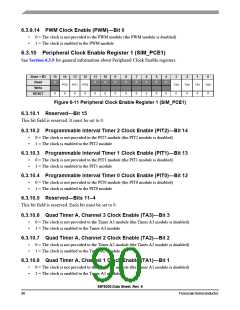
6.3.10 Peripheral Clock Enable Register 1 (SIM_PCE1)
See Section 6.3.9 for general information about Peripheral Clock Enable registers.
Base + $D
Read
15
14
PIT2
0
13
PIT1
0
12
PIT0
0
11
10
9
8
7
6
5
4
3
TA3
0
2
TA2
0
1
TA1
0
0
TA0
0
0
0
0
0
0
0
0
0
0
Write
0
0
0
0
0
0
0
0
0
RESET
Figure 6-11 Peripheral Clock Enable Register 1 (SIM_PCE1)
6.3.10.1 Reserved—Bit 15
This bit field is reserved. It must be set to 0.
6.3.10.2 Programmable Interval Timer 2 Clock Enable (PIT2)—Bit 14
•
•
0 = The clock is not provided to the PIT2 module (the PIT2 module is disabled)
1 = The clock is enabled to the PIT2 module
6.3.10.3 Programmable Interval Timer 1 Clock Enable (PIT1)—Bit 13
•
•
0 = The clock is not provided to the PIT1 module (the PIT1 module is disabled)
1 = The clock is enabled to the PIT1 module
6.3.10.4 Programmable Interval Timer 0 Clock Enable (PIT0)—Bit 12
•
•
0 = The clock is not provided to the PIT0 module (the PIT0 module is disabled)
1 = The clock is enabled to the PIT0 module
6.3.10.5 Reserved—Bits 11–4
This bit field is reserved. Each bit must be set to 0.
6.3.10.6 Quad Timer A, Channel 3 Clock Enable (TA3)—Bit 3
•
•
0 = The clock is not provided to the Timer A3 module (the Timer A3 module is disabled)
1 = The clock is enabled to the Timer A3 module
6.3.10.7 Quad Timer A, Channel 2 Clock Enable (TA2)—Bit 2
•
•
0 = The clock is not provided to the Timer A2 module (the Timer A2 module is disabled)
1 = The clock is enabled to the Timer A2 module
6.3.10.8 Quad Timer A, Channel 1 Clock Enable (TA1)—Bit 1
•
•
0 = The clock is not provided to the Timer A1 module (the Timer A1 module is disabled)
1 = The clock is enabled to the Timer A1 module
56F8036 Data Sheet, Rev. 6
90
FreescaleSemiconductor

 FREESCALE [ Freescale ]