6.3.16.3 Configure GPIOA5 (GPS_A5)—Bits 11–10
This field selects the alternate function for GPIOA5.
•
•
•
•
00 = PWM5 - PWM5 (default)
01 = FAULT2 - PWM FAULT2 Input
10 = TA3 - Timer A3
11 = Reserved
6.3.16.4 Configure GPIOA4 (GPS_A4)—Bits 9–8
This field selects the alternate function for GPIOA4.
•
•
•
•
00 = PWM4 - PWM4 (default)
01 = FAULT1 - PWM FAULT1 Input
10 = TA2 - Timer A2
11 = Reserved
6.3.16.5 Reserved—Bits 7–0
This bit field is reserved. Each bit must be set to 0.
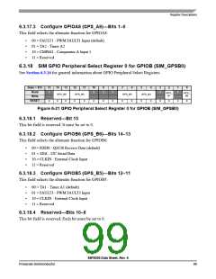
6.3.17 SIM GPIO Peripheral Select Register 1 for GPIOA (SIM_GPSA1)
See Section 6.3.16 for general information about GPIO Peripheral Select Registers.
Base + $14
Read
15
14
13
12
11
10
9
8
7
6
5
4
3
2
1
0
0
0
0
0
0
0
0
0
0
0
0
0
GPS_A9
GPS_A8
Write
0
0
0
0
0
0
0
0
0
0
0
0
0
0
0
0
RESET
Figure 6-20 GPIO Peripheral Select Register 1 for GPIOA (SIM_GPSA1)
6.3.17.1 Reserved—Bits 15–4
This bit field is reserved. Each bit must be set to 0.
6.3.17.2 Configure GPIOA9 (GPS_A9)—Bits 3–2
This field selects the alternate function for GPIOA9.
•
•
•
•
00 = FAULT2 - PWM FAULT2 Input (default)
01 = TA3 - Timer A3
10 = CMPBI1 - Comparator B Input 1
11 = Reserved
56F8036 Data Sheet, Rev. 6
98
FreescaleSemiconductor

 FREESCALE [ Freescale ]