Base + $12
Read
15
14
13
12
11
10
9
8
7
6
5
4
3
2
1
0
0
0
0
0
0
0
0
0
0
0
0
0
PCEP
GIPSP
Write
RESET
0
0
0
0
0
0
0
0
0
0
0
0
0
0
0
0
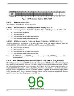
Figure 6-17 Protection Register (SIM_PROT)
6.3.15.1 Reserved—Bits 15–4
This bit field is reserved. Each bit must be set to 0.
6.3.15.2 Peripheral Clock Enable Protection (PCEP)—Bits 3–2
These bits enable write protection of all fields in the PCEn, SDn, and PCR registers in the SIM module.
•
•
•
•
00 = Write protection off (default)
01 = Write protection on
10 = Write protection off and locked until chip reset
11 = Write protection on and locked until chip reset
6.3.15.3 GPIO and Internal Peripheral Select Protection (GIPSP)—Bits 1–0
These bits enable write protection of GPSn and IPSn registers in the SIM module and write protect all
GPIOx_PEREN, GPIOx_PPOUTM and GPIOx_DRIVE registers in GPIO modules.
•
•
•
•
00 = Write protection off (default)
01 = Write protection on
10 = Write protection off and locked until chip reset
11 = Write protection on and locked until chip reset
Note:
The PWM fields in the CLKOUT register are also write protected by GIPSP. They are reserved for
in-house test only.
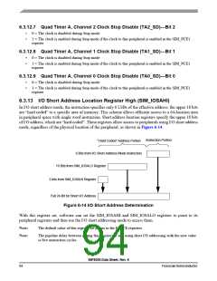
6.3.16 SIM GPIO Peripheral Select Register 0 for GPIOA (SIM_GPSA0)
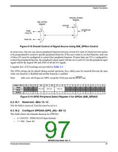
Most I/O pins have an associated GPIO function. In addition to the GPIO function, I/O can be configured
to be one of several peripheral functions. The GPIOx_PEREN register within the GPIO module controls
the selection between peripheral or GPIO control of the I/O pins. The GPIO function is selected when the
GPIOx_PEREN bit for the I/O is 0. When the GPIOx_PEREN bit of the GPIO is 1, the fields in the GPSn
registers select which peripheral function has control of the I/O. Figure 6-18 illustrates the output path to
an I/O pin when an I/O has two peripheral functions. Similar muxing is required on peripheral function
inputs to receive input from the properly selected I/O pin.
56F8036 Data Sheet, Rev. 6
96
FreescaleSemiconductor

 FREESCALE [ Freescale ]