Register Descriptions
6.3.10.9 Quad Timer A, Channel 0 Clock Enable (TA0)—Bit 0
•
•
0 = The clock is not provided to the Timer A0 module (the Timer A0 module is disabled)
1 = The clock is enabled to the Timer A0 module
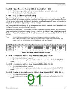
6.3.11 Stop Disable Register 0 (SD0)
By default, peripheral clocks are disabled during Stop mode in order to maximize power savings. This
register will allow an individual peripheral to operate in Stop mode. Since asserting an interrupt causes the
system to return to Run mode, this feature is provided so that selected peripherals can be left operating in
Stop mode for the purpose of generating a wake-up interrupt.
For power-conscious applications, it is recommended that only a minimum set of peripherals be
configured to remain operational during Stop mode.
Peripherals should be put in a non-operating (disabled) configuration prior to entering Stop mode unless
their corresponding Stop Disable control is set to 1. Refer to the 56F802X and 56F803XPeripheral
Reference Manual for further details. Reads and writes cannot be made to a module that has its clock
disabled.
Note:
The MSCAN module supports extended power management capabilities including Sleep,
Stop-in-Wait, and Disable modes. MSCAN clocks are selected by MSCAN control registers. For
details, refer to the 56F802X and 56F803XPeripheral Reference Manual.
Base + $E
15
14
13
12
11
10
9
8
7
6
5
4
3
2
1
0
0
0
0
0
0
0
0
Read
Write
CMPB_ CMPA_ DAC1_ DAC0_
ADC_
SD
I2C_
SD
QSCI0_
SD
QSPI0_
SD
PWM_
SD
SD
SD
SD
SD
0
0
0
0
0
0
0
0
0
0
0
0
0
0
0
0
RESET
Figure 6-12 Stop Disable Register 0 (SD0)
6.3.11.1 Comparator B Clock Stop Disable (CMPB_SD)—Bit 15
•
•
0 = The clock is disabled during Stop mode
1 = The clock is enabled during Stop mode if the clock to this peripheral is enabled in the SIM_PCE0
register
6.3.11.2 Comparator A Clock Stop Disable (CMPA_SD)—Bit 14
•
•
0 = The clock is disabled during Stop mode
1 = The clock is enabled during Stop mode if the clock to this peripheral is enabled in the SIM_PCE0
register
6.3.11.3 Digital-to-Analog Converter 1 Clock Stop Disable (DAC1_SD)—Bit 13
•
•
0 = The clock is disabled during Stop mode
1 = The clock is enabled during Stop mode if the clock to this peripheral is enabled in the SIM_PCE0
register
56F8036 Data Sheet, Rev. 6
Freescale Semiconductor
91

 FREESCALE [ Freescale ]