Register Descriptions
6.3.7.1
Reserved—Bits 15–10
This bit field is reserved. Each bit must be set to 0.
6.3.7.2
PWM3—Bit 9
•
•
0 = Peripheral output function of GPIOA[3] is defined to be PWM3
1 = Peripheral output function of GPIOA[3] is defined to be the Relaxation Oscillator Clock
6.3.7.3
PWM2—Bit 8
•
•
0 = Peripheral output function of GPIOA[2] is defined to be PWM2
1 = Peripheral output function of GPIOA[2] is defined to be the system clock
6.3.7.4
PWM1—Bit 7
•
•
0 = Peripheral output function of GPIOA[1] is defined to be PWM1
1 = Peripheral output function of GPIOA[1] is defined to be 2X system clock
6.3.7.5
PWM0—Bit 6
•
•
0 = Peripheral output function of GPIOA[0] is defined to be PWM0
1 = Peripheral output function of GPIOA[0] is defined to be 3X system clock
6.3.7.6
Reserved—Bit 5
This bit field is reserved for factory test. It must be set to 1.
6.3.7.7
Reserved—Bits 4–0
This bit field is reserved for factory test. Each bit must be set to 0.
6.3.8
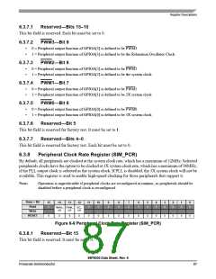
Peripheral Clock Rate Register (SIM_PCR)
By default, all peripherals are clocked at the system clock rate, which has a maximum of 32MHz. Selected
peripherals clocks have the option to be clocked at 3X system clock rate, which has a maximum of 96MHz,
if the PLL output clock is selected as the system clock. If PLL is disabled, the 3X system clock will not be
available. This register is used to enable high-speed clocking for those peripherals that support it.
Note:
Operation is unpredictable if peripheral clocks are reconfigured at runtime, so peripherals should be
disabled before a peripheral clock is reconfigured.
Base + $B
15
14
13
12
11
10
9
8
7
6
5
4
3
2
1
0
Read
Write
0
0
0
0
0
0
0
0
0
0
0
0
0
TMRA_ PWM_ I2C_
CR
CR
CR
0
0
0
0
0
0
0
0
0
0
0
0
0
0
0
0
RESET
Figure 6-9 Peripheral Clock Rate Register (SIM_PCR)
6.3.8.1
Reserved—Bit 15
This bit field is reserved. It must be set to 0.
56F8036 Data Sheet, Rev. 6
Freescale Semiconductor
87

 FREESCALE [ Freescale ]