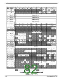
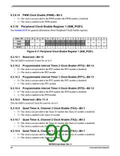
6.3.6
SIM Power Control Register (SIM_PWR)
This register controls the Standby mode of the large on-chip regulator. The large on-chip regulator derives
the core digital logic power supply from the IO power supply. At a system bus frequency of 200kHz, the
large regulator may be put in a reduced-power standby mode without interfering with device operation to
reduce device power consumption. Refer to the overview of power-down modes and the overview of clock
generation for more information on the use of large regulator standby.
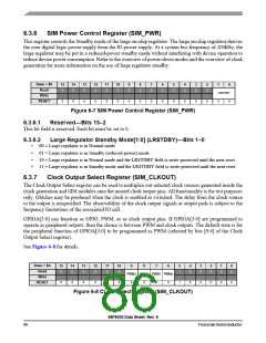
Base + $8
Read
15
14
13
12
11
10
9
8
7
6
5
4
3
2
1
0
0
0
0
0
0
0
0
0
0
0
0
0
0
0
LRSTDBY
Write
RESET
0
0
0
0
0
0
0
0
0
0
0
0
0
0
0
0
Figure 6-7 SIM Power Control Register (SIM_PWR)
6.3.6.1
Reserved—Bits 15–2
This bit field is reserved. Each bit must be set to 0.
6.3.6.2
Large Regulator Standby Mode[1:0] (LRSTDBY)—Bits 1–0
•
•
•
•
00 = Large regulator is in Normal mode
01 = Large regulator is in Standby (reduced-power) mode
10 = Large regulator is in Normal mode and the LRSTDBY field is write-protected until the next reset
11 = Large regulator is in Standby mode and the LRSTDBY field is write-protected until the next reset
6.3.7
Clock Output Select Register (SIM_CLKOUT)
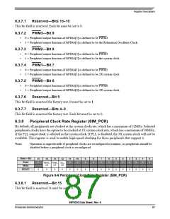
The Clock Output Select register can be used to multiplex out selected clock sources generated inside the
clock generation and SIM modules onto the muxed clock output pins. All functionality is for test purposes
only. Glitches may be produced when the clock is enabled or switched. The delay from the clock source
to the output is unspecified. The observability of the clock output signals at output pads is subject to the
frequency limitations of the associated IO cell.
GPIOA[3:0] can function as GPIO, PWM, or as clock output pins. If GPIOA[3:0] are programmed to
operate as peripheral outputs, then the choice is between PWM and clock outputs. The default state is for
the peripheral function of GPIOA[3:0] to be programmed as PWM (selected by bits [9:6] of the Clock
Output Select register).
See Figure 6-8 for details.
Base + $A
Read
15
14
13
12
11
10
9
8
7
6
5
4
3
2
1
0
0
0
0
0
0
0
1
0
0
0
0
0
PWM3 PWM2 PWM1 PWM0
Write
0
0
0
0
0
0
0
0
0
0
1
0
0
0
0
0
RESET
Figure 6-8 CLKO Select Register (SIM_CLKOUT)
56F8036 Data Sheet, Rev. 6
86
FreescaleSemiconductor

 FREESCALE [ Freescale ]