6.3.8.2
Quad Timer A Clock Rate (TMRA_CR)—Bit 14
This bit selects the clock speed for the Quad Timer A module.
•
•
0 = Quad Timer A clock rate equals the system clock rate, to a maximum 32MHz (default)
1 = Quad Timer A clock rate equals 3X system clock rate, to a maximum 96MHz
6.3.8.3
Pulse Width Modulator Clock Rate (PWM_CR)—Bit 13
This bit selects the clock speed for the PWM module.
•
•
0 = PWM module clock rate equals the system clock rate, to a maximum 32MHz (default)
1 = PWM module clock rate equals 3X system clock rate, to a maximum 96MHz
6.3.8.4
Inter-Integrated Circuit Run Clock Rate (I2C_CR)—Bit 12
2
This bit selects the clock speed for the I C run clock.
•
•
0 = I2C module run clock rate equals the system clock rate, to a maximum 32MHz (default)
1 = I2C module run clock rate equals 3X system clock rate, to a maximum 96MHz
6.3.8.5
Reserved—Bits 11–0
This bit field is reserved. Each bit must be set to 0.
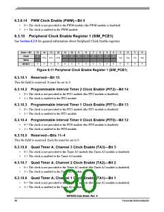
6.3.9
Peripheral Clock Enable Register 0 (SIM_PCE0)
The Peripheral Clock Enable register enables or disables clocks to the peripherals as a power savings
feature. Significant power savings are achieved by enabling only the peripheral clocks that are in use.
When a peripheral’s clock is disabled, that peripheral is in Stop mode. Accesses made to a module that has
its clock disabled will have no effect. The corresponding peripheral should itself be disabled while its clock
is shut off. IPBus writes are not possible.
Setting the PCE bit does not guarantee that the peripheral’s clock is running. Enabled peripheral clocks
will still become disabled in Stop mode, unless the peripheral’s Stop Disable control in the SDn register
is set to 1.
Note:
The MSCAN module supports extended power management capabilities, including Sleep,
Stop-in-Wait, and Disable modes. MSCAN clocks are selected by MSCAN control registers. Refer to
the 56F802X and 56F803XPeripheral Reference Manual for details.
Base + $C
15
14
13
12
11
10
9
8
7
6
5
4
3
2
1
0
0
0
0
0
0
0
0
Read
Write
CMPB CMPA DAC1 DAC0
ADC
I2C
QSCI0
QSPI0
PWM
0
0
0
0
0
0
0
0
0
0
0
0
0
0
0
0
RESET
Figure 6-10 Peripheral Clock Enable Register 0 (SIM_PCE0)
Comparator B Clock Enable (CMPB)—Bit 15
6.3.9.1
•
•
0 = The clock is not provided to the Comparator B module (the Comparator B module is disabled)
1 = The clock is enabled to the Comparator B module
56F8036 Data Sheet, Rev. 6
88
FreescaleSemiconductor

 FREESCALE [ Freescale ]