Register Descriptions
6.3 Register Descriptions
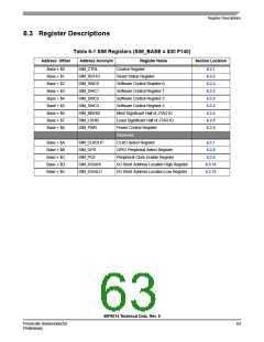
Table 6-1 SIM Registers (SIM_BASE = $00 F140)
Address Offset
Address Acronym
Register Name
Control Register
Section Location
Base + $0
Base + $1
Base + $2
Base + $3
Base + $4
Base + $5
Base + $6
Base + $7
Base + $8
SIM_CTRL
SIM_RSTAT
SIM_SWC0
SIM_SWC1
SIM_SWC2
SIM_SWC3
SIM_MSHID
SIM_LSHID
SIM_PWR
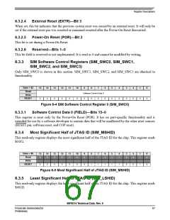
6.3.1
6.3.2
6.3.3
6.3.3
6.3.3
6.3.3
6.3.4
6.3.5
6.3.6
Reset Status Register
Software Control Register 0
Software Control Register 1
Software Control Register 2
Software Control Register 3
Most Significant Half of JTAG ID
Least Significant Half of JTAG ID
Power Control Register
Reserved
Base + $A
Base + $B
Base + $C
Base + $D
Base + $E
SIM_CLKOUT
SIM_GPS
CLKO Select Register
6.3.7
6.3.8
GPIO Peripheral Select Register
Peripheral Clock Enable Register
I/O Short Address Location High Register
I/O Short Address Location Low Register
SIM_PCE
6.3.9
SIM_IOSAHI
SIM_IOSALO
6.3.10
6.3.10
56F8014 Technical Data, Rev. 9
Freescale Semiconductor
Preliminary
63

 FREESCALE [ Freescale ]