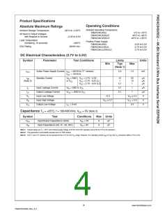
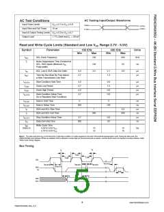
Pin Descriptions
Device Operation
The FM24C04U/05U supports a bi-directional bus oriented proto-
col. The protocol defines any device that sends data onto the bus
as a transmitter and the receiving device as the receiver. The
device controlling the transfer is the master and the device that is
controlled is the slave. The master will always initiate data
transfers and provide the clock for both transmit and receive
operations. Therefore, the FM24C04U/05U will be considered a
slave in all applications.
Serial Clock (SCL)
The SCL input is used to clock all data into and out of the device.
Serial Data (SDA)
SDA is a bi-directional pin used to transfer data into and out of the
device. It is an open drain output and may be wire–ORed with any
number of open drain or open collector outputs.
Write Protect (WP) (FM24C05U Only)
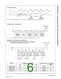
Clock and Data Conventions
If tied to V , PROGRAM operations onto the upper half (upper
CC
Data states on the SDA line can change only during SCL LOW.
SDA state changes during SCL HIGH are reserved for indicating
start and stop conditions. Refer to Figure 1 and Figure 2 on next
page.
2Kbits) of the memory will not be executed. READ operations are
possible. If tied to V , normal operation is enabled, READ/
SS
WRITE over the entire memory is possible.
Start Condition
Thisfeatureallowstheusertoassigntheupperhalfofthememory
as ROM which can be protected against accidental programming.
When write is disabled, slave address and word address will be
acknowledged but data will not be acknowledged.
All commands are preceded by the start condition, which is a
HIGH to LOW transition of SDA when SCL is HIGH. The
FM24C04U/05UcontinuouslymonitorstheSDAandSCLlinesfor
the start condition and will not respond to any command until this
condition has been met.
This pin has an internal pull-down circuit. However, on systems
where write protection is not required it is recommended that this
pin is tied to VSS
.
Stop Condition
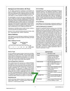
Device Selection Inputs A2, A1 and A0 (as
appropriate)
All communications are terminated by a stop condition, which is a
LOW to HIGH transition of SDA when SCL is HIGH. The stop
condition is also used by the FM24C04U/05U to place the device
in the standby power mode, except when a Write operation is
being executed, in which case a second stop condition is required
after tWR period, to place the device in standby mode.
These inputs collectively serve as “chip select” signal to an
EEPROM when multiple EEPROMs are present on the same IIC
bus. Hence these inputs, if present, should be connected to VCC
orVSS inauniquemannertoallowproperselectionofanEEPROM
amongst multiple EEPROMs. During a typical addressing se-
quence, every EEPROM on the IIC bus compares the configura-
tion of these inputs to the respective 3 bit “Device/Page block
selection” information (part of slave address) to determine a valid
selection. For e.g. if the 3 bit “Device/Page block selection” is 1-
0-1, then the EEPROM whose “Device Selection inputs” (A2, A1
and A0) are connected to VCC-VSS-VCC respectively, is selected.
Depending on the density, only appropriate numbers of “Device
Selection inputs” are provided on an EEPROM. For every “Device
selection input” that is not present on the device, the correspond-
ing bit in the “Device/Page block selection” field is used to select
a “Page Block” within the device instead of the device itself.
Following table illustrates the above:
EEPROM
Density
2k bit
Number of
Page Blocks
Device Selection Inputs
Address Bits
Selecting Page Block
None
Provided
1
2
4
8
A0
—
—
—
A1
A1
—
A2
A2
A2
—
4k bit
A0
8k bit
A0 and A1
16k bit
—
A0, A1 and A2
Note that even when just one EEPROM present on the IIC bus,
these pins should be tied to VCC or VSS to ensure proper termina-
tion.
8
www.fairchildsemi.com
FM24C04U/05U Rev. A.3

 FAIRCHILD [ FAIRCHILD SEMICONDUCTOR ]