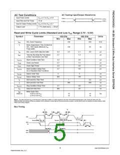
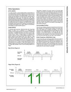
Acknowledge
Background Information (IIC Bus)
Acknowledge is an active LOW pulse on the SDA line driven by an
addressed receiver to the addressing transmitter to indicate
receipt of 8-bits of data. The receiver provides an ACK pulse for
every 8-bits of data received. This handshake mechanism is done
as follows: After transmitting 8-bits of data, the transmitter re-
leases the SDA line and waits for the ACK pulse. The addressed
receiver, if present, drives the ACK pulse on the SDA line during
the 9th clock and releases the SDA line back (to the transmitter).
Refer Figure 3.
IIC bus allows synchronous bi-directional communication be-
tween a TRANSMITTER and a RECEIVER using a Clock signal
(SCL) and a Data signal (SDA). Additionally there are up to three
Address signals (A2, A1 and A0) which collectively serve as "chip
select signal" to a device (example EEPROM) on the IIC bus.
All communication on the IIC bus must be started with a valid
START condition (by a MASTER), followed by transmittal (by the
MASTER) of byte(s) of information (Address/Data). For every byte
ofinformationreceived, theaddressedRECEIVERprovidesavalid
ACKNOWLEDGE pulse to further continue the communication
unless the RECEIVER intends to discontinue the communication.
Depending on the direction of transfer (Write or Read), the RE-
CEIVER can be a SLAVE or the MASTER. A typical IIC communi-
cation concludes with a STOP condition (by the MASTER).
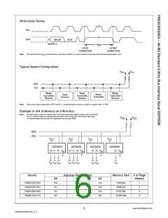
Array Address
Array address is an 8-bit information containing the address of a
memory location to be selected within a page block of the device.
16K bit Addressing Limitation:
Addressing an EEPROM memory location involves sending a
command string with the following information:
Standard IIC specification limits the maximum size of EEPROM
memory on the bus to 16K bits. This limitation is due to the
addressingprotocolimplementedwhichconsistsofthe8-bitSlave
Address and an additional 8-bit field called Array Address. This
Array Address selects 1 out of 256 locations (28=256). Since the
data format of IIC specification is 8-bit wide, a total of 256 x 8 =
2048 = 2K bits now becomes addressable by this 8-bit Array
Address. These 2K bits are typically referred as a “Page Block”.
Combining this 8-bit Array Address with the 3-bit Device/Page
address (part of Slave Address) allows a maximum of 8 pages
(23=8) of memory that can be addressed. Since each page is 2K
bits in size, 8 x 2K bits = 16K bits is the maximum size of memory
that is addressable on the Standard IIC bus. This 16Kb of memory
can be in the form of a single 16Kb EEPROM device or multiple
EEPROMs of varying density (in 2Kb multiples) to a maximum
total of 16Kb. To address the needs of systems that require more
than 16Kb on the IIC bus, a different specification called “Ex-
tended IIC Specification” is used.
[DEVICE TYPE]—[DEVICE/PAGE BLOCK SELECTION]—[R/W
BIT]—{acknowledge pulse}—[ARRAY ADDRESS]
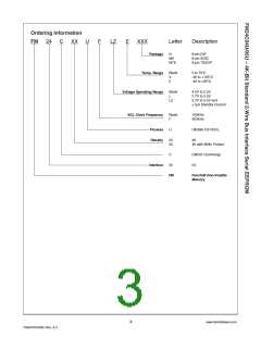
Slave Address
Slave Address is an 8-bit information consisting of a Device type
field (4bits), Device/Page block selection field (3bits) and Read/
Write bit (1bit).
Slave Address Format
Device Type
Identifier
Device/Page Block
Selection
1
0
1
0
A2
A1
A0 R/W (LSB)
Device Type
DEFINITIONS
IIC bus is designed to support a variety of devices such as RAMs,
EPROMs etc., along with EEPROMS. Hence to properly identify
various devices on the IIC bus, a 4-bit “Device Type” identifier
stringisused. ForEEPROMS, this4-bitstringis1-0-1-0. EveryIIC
device on the bus internally compares this 4-bit string to its own
“Device Type” string to ensure proper device selection.
WORD
PAGE
8 bits (byte) of data
16 sequential byte locations
starting at a 16-byte address
boundary, that may be pro-
grammed during a "page write"
programming cycle
Device/Page Block Selection
PAGE BLOCK
2048 (2K) bits organized into 16
pages of addressable memory. (8
bits) x (16 bytes) x (16 pages) =
2048 bits
Whenmultipledevicesofthesametype(e.g.multipleEEPROMS)
are present on the IIC bus, then the A2, A1 and A0 address
information bits are also used as part of the Slave Address. Every
IICdeviceonthebusinternallycomparesthis3-bitstringtoitsown
physical configuration (A2, A1 and A0 pins) to ensure proper
device selection. This comparison is in addition to the “Device
Type” comparison. In addition to selecting an EEPROM, these 3
bits are also used to select a “page block” within the selected
EEPROM. Each page block is 2Kbit (256Bytes) in size. Depend-
ing on the density, an EEPROM can contain from a minimum of 1
to a maximum of 8 page blocks (in multiples of 2) and selection of
a page block within a device is by using A2, A1 and A0 bits.
MASTER
Any IIC device CONTROLLING the
transfer of data (such as a
microprocessor)
SLAVE
Device being controlled
(EEPROMs are always considered
Slaves)
TRANSMITTER
RECEIVER
Device currently SENDING data on
the bus (may be either a Master or
Slave).
Read/Write Bit
Device currently RECEIVING data
on the bus (Master or Slave)
Last bit of the Slave Address indicates if the intended access is
Read or Write. If the bit is "1," then the access is Read, whereas
if the bit is "0," then the access is Write.
7
www.fairchildsemi.com
FM24C04U/05U Rev. A.3

 FAIRCHILD [ FAIRCHILD SEMICONDUCTOR ]