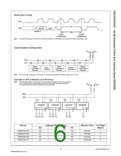
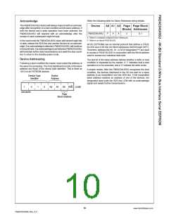
Write Operations
Page Write is initiated in the same manner as the Byte Write
operation; but instead of terminating the cycle after transmitting
the first data byte, the master can further transmit up to 15 more
bytes. After the receipt of each byte, FM24C04U/05U will respond
withanacknowledgepulse,incrementtheinternaladdresscounter
to the next address, and is ready to accept the next data. If the
master should transmit more than sixteen bytes prior to generat-
ing the STOP condition, the address counter will “roll over” and
previously written data will be overwritten. As with the Byte Write
operation, all inputs are disabled until completion of the internal
write cycle. Refer to Figure 5 for the address, acknowledge, and
data transfer sequence.
BYTE WRITE
For a write operation, a second address field is required which is a
word address that is comprised of eight bits and provides access to
any one of the 256 bytes in the selected page of memory. Upon
receipt of the byte address, the FM24C04U/05U responds with an
acknowledge and waits for the next eight bits of data, again,
responding with an acknowledge. The master then terminates the
transferbygeneratingastopconditionatwhichtimetheFM24C04U/
05Ubeginstheinternalwritecycletothenonvolatilememory.While
the internal write cycle is in progress, the FM24C04U/05U inputs
are disabled, and the device will not respond to any requests from
the master for the duration of tWR. Refer to Figure 4 for the address,
acknowledge, and data transfer sequence.
Acknowledge Polling
Once the stop condition is issued to indicate the end of the host’s
write operation, the FM24C04U/05U initiates the internal write
cycle. ACK polling can be initiated immediately. This involves
issuing thestart condition followedbythe slave addressfor a write
operation. If the FM24C04U/05U is still busy with the write
operation no ACK will be returned. If the FM24C04U/05U has
completed the write operation, an ACK will be returned and the
host can then proceed with the next read or write operation.
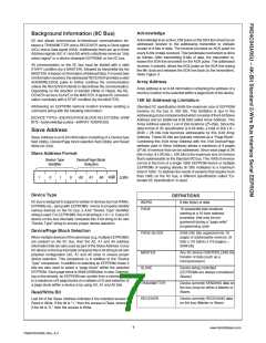
PAGE WRITE
To minimize write cycle time, FM24C04U/05U offer Page Write
feature, by which, up to a maximum of 16 contiguous byte
locations can be programmed all at once (instead of 16 individual
byte writes). To facilitate this feature, the memory array is orga-
nized in terms of “Pages.” A Page consists of 16 contiguous byte
locations starting at every 16-Byte address boundary (for ex-
ample, starting at array address 0x00, 0x10, 0x20 etc.). Page
Write operation limits access to byte locations within a page. In
other words a single Page Write operation will not cross over to
locationsonanotherpagebutwill“rollover”tothebeginningofthe
page whenever end of Page is reached and additional locations
are continued to be accessed. A Page Write operation can be
initiated to begin at any location within a page (starting address of
the Page Write operation need not be the starting address of a
Page).
Write Protection (FM24C05U Only)
Programmingoftheupperhalf(upper2Kbit)ofthememorywillnot
take place if the WP pin of the FM24C05U is connected to V
.
CC
The FM24C05U will respond to slave and byte addresses; but if
the memory accessed is write protected by the WP pin, the
FM24C05U will not generate an acknowledge after the first byte
of data has been received. Thus, the program cycle will not be
started when the stop condition is asserted.
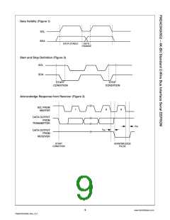
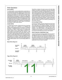
Byte Write (Figure 4)
S
T
A
R
T
S
T
O
P
SLAVE
ADDRESS
WORD
ADDRESS
Bus Activity:
Master
DATA
SDA Line
A
C
K
A
C
K
A
C
K
Bus Activity:
EEPROM
Page Write (Figure 5)
S
T
A
R
T
S
T
O
P
SLAVE
ADDRESS
Bus Activity:
Master
WORD ADDRESS (n)
DATA n
DATA n + 1
DATA n + 15
SDA Line
A
C
K
A
C
K
A
C
K
A
C
K
A
C
K
Bus Activity:
EEPROM
11
www.fairchildsemi.com
FM24C04U/05U Rev. A.3

 FAIRCHILD [ FAIRCHILD SEMICONDUCTOR ]