AC Testing Input/Output Waveforms
AC Test Conditions
Input Pulse Levels
VCC x 0.1 to VCC x 0.9
10 ns
0.9VCC
0.7VCC
0.3VCC
Input Rise and Fall Times
0.1VCC
Input & Output Timing Levels VCC x 0.3 to VCC x 0.7
Output Load 1 TTL Gate and CL = 100 pF
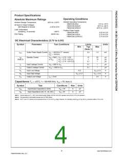
Read and Write Cycle Limits (Standard and Low VCC Range 2.7V - 5.5V)
Symbol
Parameter
100 KHz
400 KHz
Units
Min
Max
Min
Max
fSCL
TI
SCL Clock Frequency
100
100
3.5
400
KHz
ns
Noise Suppression Time Constant at
SCL, SDA Inputs (Minimum VIN
Pulse width)
50
tAA
SCL Low to SDA Data Out Valid
0.3
4.7
0.1
1.3
0.9
µs
µs
tBUF
Time the Bus Must Be Free before
a New Transmission Can Start
tHD:STA
tLOW
Start Condition Hold Time
Clock Low Period
4.0
4.7
4.0
4.7
0.6
1.5
0.6
0.6
µs
µs
µs
µs
tHIGH
Clock High Period
tSU:STA
Start Condition Setup Time
(for a Repeated Start Condition)
tHD:DAT
tSU:DAT
tR
Data in Hold Time
0
0
ns
ns
µs
ns
µs
ns
Data in Setup Time
250
100
SDA and SCL Rise Time
SDA and SCL Fall Time
Stop Condition Setup Time
Data Out Hold Time
1
0.3
tF
300
300
tSU:STO
tDH
4.7
0.6
50
300
tWR
(Note 4)
Write Cycle Time
4.5V to 5.5V VCC
2.7V to 4.5V VCC
10
15
10
15
ms
Note 4: The write cycle time (tWR) is the time from a valid stop condition of a write sequence to the end of the internal erase/program cycle. During the write cycle, the
FM24C04U/05U bus interface circuits are disabled, SDA is allowed to remain high per the bus-level pull-up resistor, and the device does not respond to its slave address. Refer
"Write Cycle Timing" diagram.
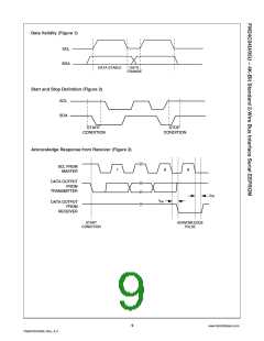
Bus Timing
t
t
R
F
t
HIGH
t
t
LOW
LOW
SCL
t
SU:STO
t
t
t
SU:DAT
SU:STA
HD:DAT
t
HD:STA
SDA
IN
t
BUF
t
t
AA
DH
SDA
OUT
5
www.fairchildsemi.com
FM24C04U/05U Rev. A.3

 FAIRCHILD [ FAIRCHILD SEMICONDUCTOR ]