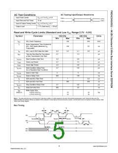
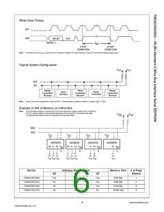
Write Cycle Timing
SCL
SDA
8th BIT
WORD n
ACK
t
WR
STOP
START
CONDITION
CONDITION
Note:
The write cycle time (tWR) is the time from a valid stop condition of a write sequence to the end of the internal erase/program cycle.
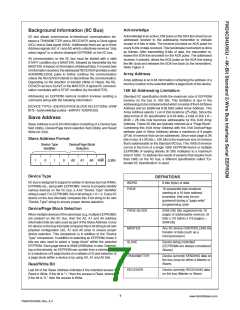
Typical System Configuration
V
V
CC
CC
SDA
SCL
Master
Transmitter/
Receiver
Slave
Transmitter/
Receiver
Master
Transmitter/
Receiver
Master
Transmitter
Slave
Receiver
Note:
Due to open drain configuration of SDA and SCL, a bus-level pull-up resistor is called for, (typical value = 4.7kΩ)
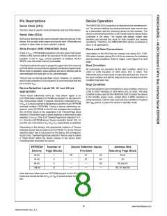
Example of 16K of Memory on 2-Wire Bus
Note:
The SDA pull-up resistor is required due to the open-drain/open collector output of IIC bus devices.
The SCL pull-up resistor is recommended because of the normal SCL line inactive 'high' state.
It is recommended that the total line capacitance be less than 400pF
V
V
CC
CC
SDA
SCL
V
V
V
V
CC
CC
CC
CC
24C02/03
24C02/03
24C04/05
24C08/09
A0 A1 A2
V
A0 A1 A2
V
A1 A2
V
A2
V
SS
SS
SS
SS
To To To
To To To
To To
To
V
V
V
V
V
V
V
V
V
SS SS SS
CC SS SS
CC SS
CC
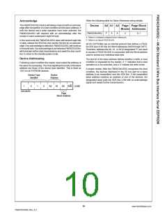
Device
Address Pins Present
A1
Memory Size # of Page
Blocks
A0
Yes
No
A2
Yes
Yes
Yes
No
FM24C02U/03U
FM24C04U/05U
FM24C08U/09U
FM24C16U/17U
Yes
Yes
No
2048 Bits
4096 Bits
8192 Bits
16,384 Bits
1
2
4
8
No
No
No
6
www.fairchildsemi.com
FM24C04U/05U Rev. A.3

 FAIRCHILD [ FAIRCHILD SEMICONDUCTOR ]