ST16C1550/51
2.97V TO 5.5V UART WITH 16-BYTE FIFO
áç
REV. 4.2.0
]
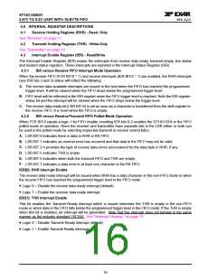
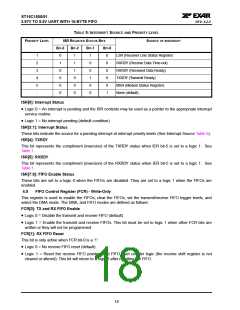
TABLE 5: INTERRUPT SOURCE AND PRIORITY LEVEL
PRIORITY LEVEL
ISR REGISTER STATUS BITS
SOURCE OF INTERRUPT
BIT-3
BIT-2
BIT-1
BIT-0
1
2
3
4
5
-
0
1
0
0
0
0
1
1
1
0
0
0
1
0
0
1
0
0
0
0
0
0
0
1
LSR (Receiver Line Status Register)
RXRDY (Receive Data Time-out)
RXRDY (Received Data Ready)
TXRDY (Transmit Ready)
MSR (Modem Status Register)
None (default)
ISR[0]: Interrupt Status
• Logic 0 = An interrupt is pending and the ISR contents may be used as a pointer to the appropriate interrupt
service routine.
• Logic 1 = No interrupt pending (default condition).
ISR[3:1]: Interrupt Status
These bits indicate the source for a pending interrupt at interrupt priority levels (See Interrupt Source Table 5).
ISR[4]: TXRDY
This bit represents the compliment (inversion) of the TXRDY status when IER bit-5 is set to a logic 1. See
Table 1.
ISR[5]: RXRDY
This bit represents the compliment (inversion) of the RXRDY status when IER bit-5 is set to a logic 1. See
Table 1.
ISR[7:6]: FIFO Enable Status
These bits are set to a logic 0 when the FIFOs are disabled. They are set to a logic 1 when the FIFOs are
enabled.
4.5
FIFO Control Register (FCR) - Write-Only
This register is used to enable the FIFOs, clear the FIFOs, set the transmit/receive FIFO trigger levels, and
select the DMA mode. The DMA, and FIFO modes are defined as follows:
FCR[0]: TX and RX FIFO Enable
• Logic 0 = Disable the transmit and receive FIFO (default).
• Logic 1 = Enable the transmit and receive FIFOs. This bit must be set to logic 1 when other FCR bits are
written or they will not be programmed.
FCR[1]: RX FIFO Reset
This bit is only active when FCR bit-0 is a ‘1’.
• Logic 0 = No receive FIFO reset (default).
• Logic 1 = Reset the receive FIFO pointers and FIFO level counter logic (the receive shift register is not
cleared or altered). This bit will return to a logic 0 after resetting the FIFO.
18

 EXAR [ EXAR CORPORATION ]