áç
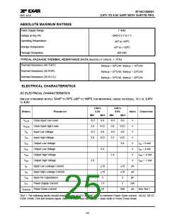
ST16C1550/51
2.97V TO 5.5V UART WITH 16-BYTE FIFO
REV. 4.2.0
When enabled, the Break control bit causes a break condition to be transmitted (the TX output is forced to a
“space’, logic 0, state). This condition remains, until disabled by setting LCR bit-6 to a logic 0.
• Logic 0 = No TX break condition (default).
• Logic 1 = Forces the transmitter output (TX) to a “space”, logic 0, for alerting the remote receiver of a line
break condition.
LCR[7]: Baud Rate Divisors Enable
Baud rate generator divisor (DLL/DLM) enable.
• Logic 0 = Data registers are selected (default).
• Logic 1 = Divisor latch registers are selected.
4.7
Modem Control Register (MCR) or General Purpose Outputs Control - Read/Write
The MCR register is used for controlling the serial/modem interface signals or general purpose inputs/outputs.
MCR[0]: DTR# Output
The DTR# pin is a modem control output. If the modem interface is not used, this output may be used as a
general purpose output.
• Logic 0 = Force DTR# output to a logic 1 (default).
• Logic 1 = Force DTR# output to a logic 0.
MCR[1]: RTS# Output
The RTS# pin is a modem control output. If the modem interface is not used, this output may be used as a
general purpose output.
• Logic 0 = Force RTS# output to a logic 1 (default).
• Logic 1 = Force RTS# output to a logic 0.
MCR[2]: OP1# Output/Soft Reset
OP1# is not available as an output pin on the 155X. But it is available for use during Internal Loopback Mode.
In the Loopback Mode, this bit is used to write the state of the modem RI# interface signal.
• Logic 0 = OP1# output (RI# input) is at logic 1 (default).
• Logic 1 = OP1# output (RI# input) is at logic 0.
In normal operation, this bit is associated with the RST (buffered reset) output pin. The logical state of the RST
pin will follow exactly the logical state of the RESET pin. When IER bit-5 = 1, soft resets from MCR bit-2 are
ORed with the state of the RESET input pin. Therefore both reset types will be seen at the RST pin. Note that
asserting MCR bit-2 does not reset the 155X.
• Logic 0 = The RST output pin is a logic 0 (default).
• Logic 1 = The RST output pin is a logic 1.
MCR[3]: OP2# or INT Output Enable
When not in Internal Loopback Mode:
• Logic 0 = INT output is three-state (default).
• Logic 1 = INT output is active high.
OP2# is not available as an output pin on the 155X. But it is available for use during Internal Loopback Mode.
In the Loopback Mode, this bit is used to write the state of the modem CD# interface signal.
• Logic 0 = OP2# output (CD# input) is a logic 1 (default).
• Logic 1 = OP2# output (CD# input) is a logic 0.
MCR[4]: Internal Loopback Enable
• Logic 0 = Disable loopback mode (default).
21

 EXAR [ EXAR CORPORATION ]