EMD3D256M08BS1
EMD3D256M16BS1
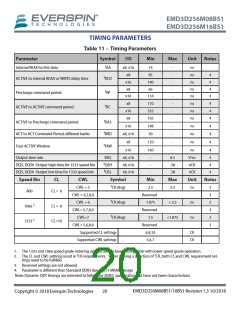
TIMING PARAMETERS
Table 11 – Timing Parameters
Parameter
Symbol
I/O
Min
Max
Unit
Notes
t
Internal READ to first data
AA
x8, x16
x8
14
95
-
-
-
-
-
ns
ns
ns
ns
ns
4
4
4
4
t
ACTIVE to internal READ or WRITE delay time
Precharge command period
RCD
x16
x8
190
66
t
RP
x16
134
x8
x16
170
332
103
198
30
-
-
-
-
-
ns
ns
ns
ns
ns
4
4
4
4
4
t
ACTIVE to ACTIVE command period
RC
x8
t
ACTIVE to Precharge command period
ACT to ACT Command Period, different banks
Four ACTIVE Window
RAS
x16
t
RRD
x8, x16
x8
120
-
ns
4
t
FAW
x16
160
-
-
8.5
ns
V/ns
nCK
nCK
Unit
ns
4
Output slew rate
SRQ
x8, x16
x8, x16
x8, x16
4
t
DQS, DQS# Output high time for 1333 speed bin
DQS, DQS# Output low time for 1333 speed bin
QSH
-
.38
4
t
QSL
-
.38
4
Speed Bin
CL
CWL
CWL = 5
Symbol
Min
2.5
Max
3.3
Notes
t
t
t
CK (Avg)
2
3
2
3
2
3
800
CL = 6
CWL = 6,7,8,9
CWL = 6
Reserved
1.875
Reserved
1.5
CK (Avg)
CK (Avg)
< 2.5
ns
ns
1
1066
CL = 8
CL=10
CWL= 5,7,8,9
CWL=7
<1.875
1
1333
CWL= 5,6,8,9
Reserved
6,8,10
5,6,7
Supported CL settings
Supported CWL settings
CK
CK
1. The 1333 and 1066 speed grade ordering options are backward compatible with lower speed grade operation.
t
t
2. The CL and CWL settings result in CK requirements. When making a selection of CK, both CL and CWL requirement set-
tings need to be fulfilled.
3. Reserved settings are not allowed.
4. Parameter is different than Standard DDR3 due to STT-MRAM design
Note: Dynamic ODT timings are intended to follow the JEDEC specification but have not been characterized.
EMD3D256M08BS1/16BS1 Revision 1.3 10/2018
Copyright © 2018 Everspin Technologies
20

 EVERSPIN [ Everspin Technologies ]