Page 76
Epson Research and Development
Vancouver Design Center
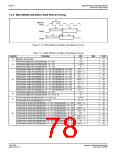
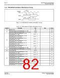
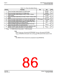
7.3.5 FPM-DRAM CAS Before RAS Refresh Timing
t1
Memory
Clock
t2
t3
RAS#
t4
t5
t6
CAS#
Figure 7-18: FPM-DRAM CAS Before RAS Refresh Timing
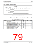
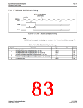
Table 7-18: FPM-DRAM CAS Before RAS Refresh Timing
Symbol
Parameter
Min
40
Max
Units
ns
t1
Memory clock
RAS# precharge time (REG[02Ah] bits 1-0 = 00)
2.45 t1
1.45 t1
ns
t2
RAS# precharge time (REG[02Ah] bits 1-0 = 01 or 10)
ns
RAS# pulse width (REG[02Bh] bits 1-0 = 00,
REG[02Ah] bits 1-0 = 00)
2.45 t1 - 7
3.45 t1 - 7
1.45 t1 - 7
2.45 t1 - 7
0.45 t1 - 7
1.45 t1 - 7
ns
ns
ns
ns
ns
ns
RAS# pulse width (REG[02Bh] bits 1-0 = 00,
REG[02Ah] bits 1-0 = 01 or 10)
RAS# pulse width (REG[02Bh] bits 1-0 = 01,
REG[02Ah] bits 1-0 = 00)
t3
RAS# pulse width (REG[02Bh] bits 1-0 = 01,
REG[02Ah] bits 1-0 = 01 or 10)
RAS# pulse width (REG[02Bh] bits 1-0 = 10,
REG[02Ah] bits 1-0 = 00)
RAS# pulse width (REG[02Bh] bits 1-0 = 10,
REG[02Ah] bits 1-0 = 01 or 10)
CAS# precharge time (REG[02Ah] bits 1-0 = 00)
2 t1
t1
ns
ns
ns
t4
t5
CAS# precharge time (REG[02Ah] bits 1-0 = 01 or 10)
0.45 t1
CAS# setup time
CAS# hold to RAS# (REG[02Bh] bits 1-0 = 00,
REG[02Ah] bits 1-0 = 00)
2.45 t1 - 4
3.45 t1 - 4
1.45 t1 - 4
2.45 t1 - 4
0.45 t1 - 4
1.45 t1 - 4
ns
ns
ns
ns
ns
ns
CAS# hold to RAS# (REG[02Bh] bits 1-0 = 00,
REG[02Ah] bits 1-0 = 01 or 10)
CAS# hold to RAS# (REG[02Bh] bits 1-0 = 01,
REG[02Ah] bits 1-0 = 00)
t6
CAS# hold to RAS# (REG[02Bh] bits 1-0 = 01,
REG[02Ah] bits 1-0 = 01 or 10)
CAS# hold to RAS# (REG[02Bh] bits 1-0 = 10,
REG[02Ah] bits 1-0 = 00)
CAS# hold to RAS# (REG[02Bh] bits 1-0 = 10,
REG[02Ah] bits 1-0 = 01 or 10)
S1D13506
X25B-A-001-10
Hardware Functional Specification
Issue Date: 01/02/06

 EPSON [ EPSON COMPANY ]