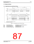
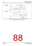
Page 80
Epson Research and Development
Vancouver Design Center
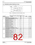
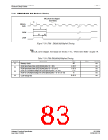
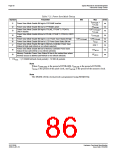
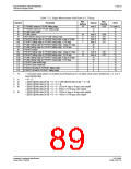
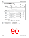
Table 7-21: Power Save Mode Timing
Symbol
Parameter
Min
Max
Units
ns
TFPFRAME
TFPLINE
+
t1
t2
t3
Power Save Mode Enable Bit high to FPFRAME inactive
Power Save Mode Enable Bit low to FPFRAME active
3TFPLINE
ns
Power Save Mode Enable Bit high to FPLINE, FPSHIFT, FPDATA,
DRDY inactive
129TFPFRAME
TFPLINE
+
ns
Power Save Mode Enable Bit low to FPLINE, FPSHIFT, FPDATA, DRDY
active
t4
TFPFRAME
ns
t5
t6
Power Save Mode Enable Bit high to LCD Power Save Status Bit high
Power Save Mode Enable Bit low to LCD Power Save Status Bit low
128TFPFRAME
129TFPRAME
TPCLK
ns
ns
Power Save Mode Enable Bit high to Memory Controller Power Save
Status Bit high (self-refresh or no refresh selected)
t7
t8
t9
note 1
12TMCLK
8TMCLK
ns
ns
ns
Power Save Mode Enable Bit low to Memory Controller Power Save
Status Bit low (self-refresh or no refresh selected)
Memory Controller Power Save Status Bit low to the earliest time where
memory access is allowed (self-refresh or no refresh selected)
1. t14max = (1 DRAM refresh clock period) + 12 MCLK periods
Note
Where T
is the period of FPFRAME, T
is the period of FPLINE,
FPLINE
FPFRAME
T
is the period of the pixel clock, and T
is the period of the memory clock.
PCLK
MCLK
Note
The DRAM refresh clock period is programmed using REG[021h].
S1D13506
X25B-A-001-10
Hardware Functional Specification
Issue Date: 01/02/06

 EPSON [ EPSON COMPANY ]