Page 78
Epson Research and Development
Vancouver Design Center
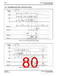
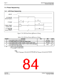
7.4 Power Sequencing
7.4.1 LCD Power Sequencing
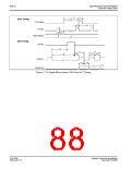
#RESET
LCD Enable Bit
(REG[1FCh] bit 0)
t2
t1
FPFRAME
t4
t3
FPLINE, FPSHIFT
FPDATA, DRDY
LCD Power Save
Status Bit
t4
(REG[1F1h] bit 1)
Figure 7-20: LCD Panel Power-off/Power-on Timing
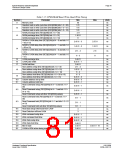
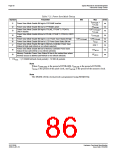
Table 7-20: LCD Panel Power-off/Power-on Timing
Symbol
Parameter
Min
Max
Units
ns
t1
t2
t3
LCD Enable Bit high to FPFRAME active
TFPFRAME
5TFPFRAME
3TFPLINE
FPFRAME inactive to LCD Power Save Status bit high
LCD Enable Bit high to FPLINE, FPSHIFT, FPDATA, DRDY active
ns
ns
LCD Enable Bit low to FPLINE, FPSHIFT, FPDATA, DRDY active and
LCD Power Save Status bit high
t4
note 1
ns
1. t4
= 130TFPFRAME for dual panels
= 65TFPFRAME for single panels
Note
Where T
is the period of FPFRAME and T
is the period of FPLINE.
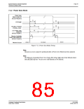
FPFRAME
FPLINE
S1D13506
X25B-A-001-10
Hardware Functional Specification
Issue Date: 01/02/06

 EPSON [ EPSON COMPANY ]