PDF
最近搜索
热门搜索
发布采购

| 型号: | S1D13506 |
| PDF下载: | 下载PDF文件 查看货源 |
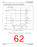
| 内容描述: | S1D13506彩色LCD / CRT / TV控制器 [S1D13506 Color LCD/CRT/TV Controller] |
| 分类和应用: | 电视控制器 |
| 文件页数/大小: | 696 页 / 5934 K |
| 品牌: |  EPSON [ EPSON COMPANY ] EPSON [ EPSON COMPANY ] |
专业IC领域供求交易平台:提供全面的IC Datasheet资料和资讯,Datasheet 1000万数据,IC品牌1000多家。