Page 48
Epson Research and Development
Vancouver Design Center
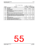
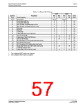
7 A.C. Characteristics
Conditions:
V
= 3.0V ± 10% and V = 5.0V ± 10%
DD DD
T = -40° C to 85° C
A
T
and T for all inputs must be < 5 ns (10% ~ 90%)
rise
fall
C = 50pF (CPU Interface), unless noted
L
C = 100pF (LCD Panel Interface)
L
C = 10pF (Display Memory Interface)
L
C = 10pF (CRT Interface)
L
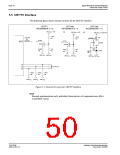
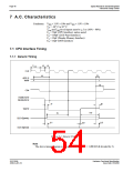
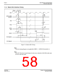
7.1 CPU Interface Timing
7.1.1 Generic Timing
TCLK
t2
t3
CLK
t5
t4
A[20:1]
M/R#
t6
CS#
RD0#,RD1#
WE0#,WE1#
t7
t8
WAIT#
D[15:0](write)
D[15:0](read)
t10
t9
t11
t13
t12
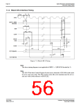
Figure 7-1: Generic Timing
Note
The above timing diagram is not applicable if MD12 = 1 (BUSCLK divided by 2).
S1D13506
X25B-A-001-10
Hardware Functional Specification
Issue Date: 01/02/06

 EPSON [ EPSON COMPANY ]