Epson Research and Development
Page 53
Vancouver Design Center
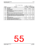
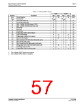
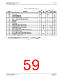
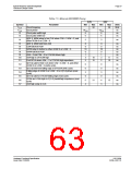
Table 7-3: Hitachi SH-3 Timing
3.0V1
Max
5.0V2
Max
Symbol
Parameter
Min
Min
Units
MHz
ns
fCKIO
TCKIO
t2
Clock frequency
66
66
Clock period
1/fCKIO
1/fCKIO
Clock pulse width low
Clock pulse width high
6
6
4
0
4
3
3
3
2
3
4
0
0
0
6
3
6
6
3
0
3
2
3
2
1
2
3
0
0
0
3
2
ns
t3
ns
t4
A[20:1], M/R#, RD/WR# setup to CKIO
A[20:1], M/R#, RD/WR# hold from CSn#
BS# setup
ns
t5
ns
t6
ns
t7
BS# hold
ns
t8
CSn# setup
ns
t9
Falling edge RD# to D[15:0] driven
Rising edge CSn# to WAIT# tri-state
Falling edge CSn# to WAIT# driven
CKIO to WAIT# delay
ns
t10
t11
t12
t13
t14
t15
t16
t17
10
16
20
6
ns
10
13
ns
ns
D[15:0] setup to 2nd CKIO after BS# (write cycle)
ns
D[15:0] hold (write cycle)
ns
D[15:0] valid to WAIT# rising edge (read cycle)
Rising edge RD# to D[15:0] tri-state (read cycle)
CSn# high setup to CKIO
ns
30
15
ns
ns
1. Two software WAIT states are required when fCKIO is greater than 33MHz.
2. One software WAIT state is required when fCKIO is greater than 33MHz.
Hardware Functional Specification
Issue Date: 01/02/06
S1D13506
X25B-A-001-10

 EPSON [ EPSON COMPANY ]