Epson Research and Development
Page 51
Vancouver Design Center
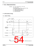
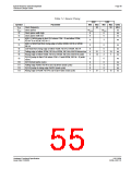
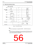
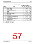
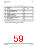
Table 7-2: Hitachi SH-4 Timing
3.0V1
Max
5.0V2
Max
Symbol
Parameter
Min
Min
Units
fCKIO
TCKIO
t2
Clock frequency
0
66
0
66
MHz
Clock period
1/fCKIO
1/fCKIO
Clock pulse width low
Clock pulse width high
6
6
4
0
4
3
3
3
4
3
4
0
0
0
6
3
3
16
6
3
0
3
2
2
3
3
2
3
0
0
0
3
2
2
ns
ns
ns
ns
ns
ns
ns
ns
ns
ns
ns
ns
ns
ns
ns
ns
ns
t3
t4
A[20:1], M/R#, RD/WR# setup to CKIO
A[20:1], M/R#, RD/WR# hold from CSn#
BS# setup
t5
t6
t7
BS# hold
t8
CSn# setup
t9
Falling edge RD# to D[15:0] driven
CKIO to RDY# high
t10
t11
t12
t13
t14
t15
t16
t17
t18
21
11
20
13
7
Falling edge CSn# to RDY# driven
CKIO to RDY# delay
D[15:0] setup to 2nd CKIO after BS# (write cycle)
13
D[15:0] hold (write cycle)
D[15:0] valid to RDY# falling edge (read cycle)
Rising edge RD# to D[15:0] tri-state (read cycle)
CSn# high setup to CKIO
30
14
16
10
Falling edge CKIO to RDY# tri-state
1. Two software WAIT states are required.
2. One software WAIT state is required.
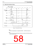
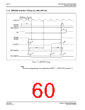
Hardware Functional Specification
Issue Date: 01/02/06
S1D13506
X25B-A-001-10

 EPSON [ EPSON COMPANY ]