Epson Research and Development
Page 47
Vancouver Design Center
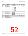
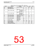
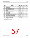
Table 6-5: Electrical Characteristics for VDD = 3.0V typical
Symbol
IDDS
Parameter
Quiescent Current
Condition
Min
Typ
Max
260
Units
Quiescent Conditions
uA
µA
µA
IIZ
Input Leakage Current
Output Leakage Current
-1
-1
1
1
IOZ
VDD = min
IOL
=
-1.8mA (Type1),
-3.5mA (Type2)
-5mA (Type3)
VOH
High Level Output Voltage
Low Level Output Voltage
VDD - 0.3
V
V
VDD = min
IOL
=
1.8mA (Type1),
3.5mA (Type2)
5mA (Type3)
VOL
0.3
VIH
VIL
High Level Input Voltage
Low Level Input Voltage
CMOS level, VDD = max 2.0
CMOS level, VDD = min
V
V
0.8
2.3
CMOS Schmitt,
VDD = 3.0V
VT+
VT-
High Level Input Voltage
Low Level Input Voltage
Hysteresis Voltage
V
V
V
CMOS Schmitt,
0.5
VDD = 3.0V
CMOS Schmitt,
0.1
VH1
VDD = 3.0V
RPD
CI
Pull Down Resistance
VI = VDD
100
200
400
12
kΩ
pF
pF
pF
Input Pin Capacitance
CO
CIO
Output Pin Capacitance
Bi-Directional Pin Capacitance
12
12
Hardware Functional Specification
Issue Date: 01/02/06
S1D13506
X25B-A-001-10

 EPSON [ EPSON COMPANY ]