Epson Research and Development
Page 43
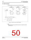
Vancouver Design Center
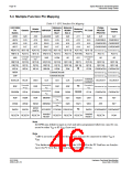
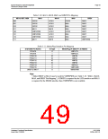
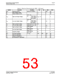
Table 5-10: MA11, MA10, MA9, and DRDY Pin Mapping
MD14, MD7, MD6
MA11
MA10
MA9
DRDY
000
001
010
011
100
101
110
111
GPIO2
GPIO1
GPIO1
GPIO1
MA10
GPIO3
MA9
DRDY
DRDY
DRDY
DRDY
DRDY
DRDY
DRDY
GPIO2
GPIO2
MA11
MA9
MA9
VMPEPWR
VMPEPWR
VMPEPWR
MA11
GPIO1
GPIO1
GPIO1
MA10
GPIO3
MA9
MA9
MA9
VMPEPWR
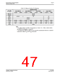
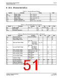
Table 5-11: MediaPlug Interface Pin Mapping
S1D13506 Pin Names
IO Type
MediaPlug I/F (MD13=1 at RESET)
FPDAT8
FPDAT9
O
I
VMPLCTL
VMPRCTL
VMPD0
FPDAT10
FPDAT11
FPDAT12
FPDAT13
FPDAT14
FPDAT15
DRDY or MA111
IO
IO
IO
IO
O
VMPD1
VMPD2
VMPD3
VMPCLK
VMPCLKN
VMPEPWR
O
O
Note
1
Either DRDY or MA11 may be used for VMPEPWR (see Table 5-10: “MA11, MA10,
MA9, and DRDY Pin Mapping”). If DRDY is required by the LCD interface and MA11
is required by the DRAM interface then VMPEPWR is not available.
Hardware Functional Specification
Issue Date: 01/02/06
S1D13506
X25B-A-001-10

 EPSON [ EPSON COMPANY ]