Epson Research and Development
Page 39
Vancouver Design Center
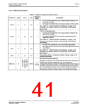
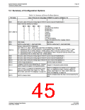
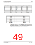
5.3 Summary of Configuration Options
Table 5-6: Summary of Power-On/Reset Options
Pin Name
value of this pin at rising edge of RESET# is used to configure:(1/0)
1
0
MD0
Not used, value of this pin at rising edge of RESET# can be read at REG[00Ch] bit 0
Select Host Bus Interface as follows:
MD11 MD3
MD2
MD1
Host Bus
0
0
0
0
0
0
0
0
1
0
0
0
0
1
1
1
1
1
0
0
1
1
0
0
1
1
1
0
1
0
1
0
1
0
1
1
SH-4/SH-3 Bus interface
MC68K Bus 1
MC68K Bus 2
Generic
Reserved
MIPS/ISA
PowerPC
PC Card (PCMCIA)
MD11,MD[3:1]
Philips PR31500/PR31700 / Toshiba TX3912
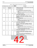
MD4
MD5
Little Endian
Big Endian
WAIT# is active high (1 = insert wait state)
WAIT# is active low (0 = insert wait state)
Memory Address/GPIO configuration:
(See Table 5-10:, “MA11, MA10, MA9, and DRDY Pin Mapping,” on page 43)
00 = symmetrical 256K×16 DRAM. MA[8:0] = DRAM address. MA[11:9] can be used as GPIO2,1,3 pins.
01 = symmetrical 1M×16 DRAM. MA[9:0] = DRAM address. MA[11:10] can be used as GPIO2,1 pins.
10 = asymmetrical 256K×16 DRAM. MA[9:0] = DRAM address. MA[11:10] can be used as GPIO2,1 pins.
11 = asymmetrical 1M×16 DRAM. MA[11:0] = DRAM address.
MD[7:6]
MD8
Not used, value of this pin at rising edge of RESET# can be read at REG[00Dh] bit 0
Not used, value of this pin at rising edge of RESET# can be read at REG[00Dh] bit 1
Not Used, value of this pin at rising edge of RESET# can be read at REG[00Dh] bit 2
MD9
MD10
MD12
BUSCLK input divided by 2
BUSCLK input not divided
Configure FPDAT[15:8] for MediaPlug I/F. External
latches required to support 16-bit passive panels.
MD13
MD14
MD15
Support 16-bit passive panels directly
DRDY is configured as a normal LCD I/F output pin.
MA11 is configured as either a memory address or
GPIO2. (See Table 5-10:, “MA11, MA10, MA9, and
DRDY Pin Mapping,” on page 43)
DRDY or MA11 is configured as MediaPlug power
down pin (VMPEPWR). (See Table 5-10:, “MA11,
MA10, MA9, and DRDY Pin Mapping,” on page 43)
WAIT# is tristated when the chip is not accessed by the
host
WAIT# is always driven
Hardware Functional Specification
Issue Date: 01/02/06
S1D13506
X25B-A-001-10

 EPSON [ EPSON COMPANY ]